Citation: Saravanan S, et al. Studies on the Effect of Texture Additive in Silicon Solar Cells. Nanomed Nanotechnol 2017, 2(2): 000117.
*Corresponding author: Saravanan S, National Centre for Photovoltaic Research and Education, Indian Institute of Technology Bombay, Mumbai - 400 076, India, Tel: +91 96112 22788; Email: shrisharavanan@yahoo.co.uk
Fabrication of high efficiency silicon solar cells with low cost is an important measure in silicon solar cell production. Silicon solar cell industries and technologists have started using alternate or advanced materials in conventional silicon solar cell process to enhance the electrical performance without compromising the quality and cost of the cell. Among the alternate materials, texture additives and metallization products play a significant role in solar cell production because it enhances the performances with lower cost or the cost at par in production. Industries deal with alkali texturization use either only IPA or IPA with texture additive as a wetting material for uniform texturization and thus reduce reflection and increase absorption of incident light. The influence of surface morphology on the solar cell parameters is essential for further improving cell efficiency. In this work, we report the optimization of texturization process by replacing IPA concentration by a texture additive without IPA. The process optimization with respect to time and concentration will be presented. Optical and morphological studies on wafers processed with IPA and IPA free texture additive has been carried out and interpreted with electrical performance. It is found that within the pyramid size studied here, there is no significant variation in reflectance and the short-circuit current. However, fill factor, open-circuit voltage and efficiency are significantly impacted by the pyramid size and height distribution. While cells with KOH/Texture additive texturization gives high fill factor (>79%), it is proved that an average fill factor gain of up to 1% absolute can be achieved by using the KOH/TA texturization process.
Keywords: Reflectance; Texture Additives; Optimization; Efficiency
Crystalline silicon solar cells have played a significant role in photovoltaic (PV) industries for the last few decades due to its ease of process and the matured technology [1-7]. Though it has been a matured technology, it has umpteen of opportunities to refine the process and thus to enhance the performance. Silicon PV researchers and industries are working to achieve the high efficiency silicon solar cells with lower costs by optimizing the processes [8-14]. Eventually the objective is to reduce the losses such as optical losses and electrical resistance losses which contribute to the reduced conversion efficiency. Hence, PV industries use advanced metallization products [15] to reduce the electrical loss; and antireflective coatings [16] with surface texturing [17] to reduce the optical losses. The surface texturing has been achieved by different ways [18] such as chemical etching, plasma etching and mechanical engraving. Most of the PV industries use the chemical etching due to its lower costs of operations. Owing to the processes’ involved in growing and wafering the silicon, as sawn silicon wafers exhibit surface damage and presence of impurities which has to be removed during chemical etching. Saw damage removal, cleaning, texturization are the steps involved in chemical etching. Conventional chemical etching involves hot alkali based cleaning and texturing with iso-propyl alcohol (IPA). Texturization is one of the key steps in silicon solar cell process which aims to enhance the light trapping and it attract the attention of researchers as the thickness of the wafers used in solar cell production decreases in order to save silicon [19]. Earlier conventional silicon cell process use KOH or NaOH with IPA in a suitable volume for the texturization and gradually texture additives along with IPA has been used as a wetting material for uniform texturization [20]. However industries want to get rid of IPA and thus chemists along with PV experts developed IPA free texture additive for uniform texturization. This paper presents optimization of the texture process using commercially available IPA free texture additive for the better electrical performance. The optimization using texture additive has been carried out by varying the etch time and additive volume fraction and is compared with IPA based texture process. UV–VIS studies were carried out to determine the reflectance and morphological studies were done to reveal the texture uniformity.
Systematic investigations on all these studies were carried out and the results are interpreted. Finally we report electrical studies of mono crystalline silicon solar cells fabricated by using wafers textured with the optimised texture additive recipe.
Process FlowP - type Boron doped solar grade single crystalline silicon wafers of size 125 X 125 mm with bulk resistivity in the range of 0.5 – 3.0 ohm/sq and thickness around 190 ± 10µ were taken as a starting material for the solar cell fabrication. These silicon wafers were processed in the conventional industrial silicon solar cell process flow shown in (Figure 1). In brief, as per the process flow, initially the saw damages, which happens during the sawing of ingots into wafers and the residual contamination of the wafers were removed by the alkali etching followed by the alkali texturization to form the uniform homogeneous pyramids with crystal orientation <111> from <100>. Consequently, the p type wafers were crafted as pn junction by diffusing phosphorus in tube furnace employing POCl3 as precursor. Sheet resistance of n layer (emitter) is in the range of 40 - 45 Ω/. The PSG formed during the diffusion at the edges and also at the surface of the silicon wafers, were removed by plasma edge isolation and with HF wash respectively. In order to make use of maximum incident light and for the hydrogen passivation, SiNx was coated of thickness ~ 80 nm and refractive index ~ 2.01 by employing PECVD technique. The front and back contacts were made by using conventional screen printing technique and fired to realize the ohmic contacts. Electrical characteristic of the solar cells were measured under the AM1.5G simulated solar radiation at 250C.
ExperimentIn order to optimize IPA free texture process to fabricate silicon solar cells, volume fractions of texture additive and process time in texturization process were treated as process variables in our experiments. The recommended process recipe of the vendor was tried along with other conditions so as to understand the best conditions to use these additives. The conventional process discussed elsewhere [9,20] was used for fabricating control cells. Labelling of wafers processed with texture additive of different volume fractions at constant process time and wafers processed with different process time at constant volume fractions are tabulated in Table 1. Reflectance studies on wafers processed with and without texture additives were carried out in a wavelength range from 300-1150 nm. Texture uniformity and surface morphology of the wafers processed with and without additives were carried out by employing Zeta 3D microscope and scanning electron microscopy (SEM). The wafers were then processed to fabricate complete solar cells. Electrical studies on cells fabricated with and without additives were carried out using a class AAA sun simulator.
Results and DiscussionReflectance Studies
Total weighted reflectance (TWR) of wafers processed with texture additive of different volume fractions at constant process time and temperature is shown in Figure 2. Reflectance of different volume fractions (Table 1) is compared with the control wafer i.e. wafer processed with IPA. From Figure 1 it has been observed that the total weighted reflectance of wafers processed with texture additive of 0.3% volume fraction at 18 minutes and 80oC (Sample C) shows better results compared with rest of the volume fractions. Also the TWR is comparable with the control wafers which are processed with IPA. It is important to mention here that the control wafers were processed with process time of 40 minutes. Hence it has been decided to evaluate the process time of texture additive based process by keeping texture additive volume fraction 0.3% as constant at 80oC. Figure 3 Shows the total weighted reflectance of wafers processed with different process time and it has been observed that the TWR of the wafers processed at 18 minutes and 80oC with texture additive volume fraction of 0.3% is 11.9 % which is comparable with the control wafers (11.7%). The lowest reflectance obtained is around 10-11% in a wavelength range of 800–1000 nm. Hence the front surface reflectance can also be controlled by optimizing the height and size of the pyramid structures formed during the process.
Surface Studies
Pyramid size and height of the wafers processed with texture additive of different volume fractions at constant process time is as shown in Figure 4 and Figure 5, respectively. The histogram indicates the pyramid base size and pyramid height of process expressed in terms of number of counts in a field of view of 473 µm x 355 µm. At 18 minutes with different volume fractions of texture additive, uniform surface pyramids are formed. From Figure 4, it has been observed that the pyramid size of the entire wafers processed with texture additive of different volume fractions at constant time is in the range of 1 µm to 5 µm. Also it is seen that size of more number of pyramids is around 2.5 µm which reveals that the pyramids are at the optimal size for almost all the volume fractions. However the pyramid height is not so uniform and scattered range in height with respect to volume fractions. But it is good that the height is below 5 µm for all the volume fractions. As the concentration increases, the pyramid height remains in the same range as the surface gets covered further with smaller pyramids which don’t change the average height. From Figure 5 it is well understood that the distribution of pyramid height is narrow in Sample C. Also the sample C has the minimum reflectivity. Hence it has been considered that the wafers processed at 18 minutes and 80oC with texture additive volume fraction of 0.3% is the optimized volume fraction recipe.
In order to justify the volume fraction it is important to optimize the process time. According to that, the trial has been planned by keeping texture additive volume fraction of 0.3% as constant and vary the etch time (Table 1). Figure 6 Shows the pyramid size of wafers processed with different process time is in the range of 1-5 µm. As the process time increases, the pyramid size essentially remains in the same range. However at 16 &18 minutes the pyramid size is optimal and the surface has minimal reflectivity as compared to rest of the samples. At extreme etch times, when the entire surface is covered with pyramids, the average height of the pyramids is drastically reduced, since there is a larger number of smaller micro-pyramids covering the surface. Available literatures [21] reported that the average pyramid height initially increases until certain of etch time and then it decreases as the etch time increases beyond threshold. In case of 16 minutes, though the pyramid size distribution is optimal, the distribution of pyramid height is not so optimal. It has been found that the optimal pyramid coverage of the wafer surface is achieved around 18 minutes.
Pyramid size and height of the wafers processed with optimised texture additive recipe is compared with control and is shown in Figure 7. From the figure it is well clear that pyramid size is small and lies in the range of 1-4 µm for the wafers processed with texture additive process whereas for the control process it lies in 1-5 µm. Similarly the pyramid height distribution is large in the control process, while in the case of wafers processed with texture additive is narrower. In order to confirm the texture uniformity of wafers processed with optimized texture additive process recipe, surface morphology studies of wafers were carried out by using SEM (Figure 8) and is compared with control. The uniformity of texturing and the pyramid size/height were analyzed by SEM at relatively low and higher magnification. From Figure 8 it is seen that the pyramid size is smaller in wafers processed with texture additive compared to control. Average pyramid size and height of wafers processed with texture additive is 2 µm and 2.75 µm whereas 2.88 µm and 4.38 µm for control wafers.
Electrical StudiesTable 2 shows the electrical parameters of monocrystalline silicon solar cells with and without texture additive. It is evident from the Table 2 that all electrical parameters of solar cell fabricated using optimised texture additive process are higher than the control in all the trials and the improvements were consistent. This may be due to presence of pyramids of slightly smaller size on the textured surface compared to IPA based texturization. The cells processed with textured additive shown the best combination of performance parameters including efficiency of the cell. Open circuit voltage of the cell is 614.68mV and short circuit current density is 33.79mA/cm2. From Table 2 is seen that the increase in efficiency of cells with different textured surfaces basically comes from the variation in Voc and Jsc, which are mainly texturing condition-dependent parameter of the cell.
ConclusionFinancial support of MNRE, Govt of India, under the auspices of National Centre for Photovoltaic Research and Education at IITB is gratefully acknowledged. Authors thank Prof. Anil Kottantharayil, Prof. Chetan Singh Solanki, Prof. K. L Narasimhan and Prof B. M. Arora for guidance and encouragement. Authors thank Hemant K Singh, Dr. Diksha, Dr Ashok and facility team for their support. Authors thank Peter Kunze, GP Solar for providing the texture additives.
AcknowledgementFinancial support of MNRE, Govt of India, under the auspices of National Centre for Photovoltaic Research and Education at IITB is gratefully acknowledged. Authors thank Prof. Anil Kottantharayil, Prof. Chetan Singh Solanki, Prof. K. L Narasimhan and Prof B. M. Arora for guidance and encouragement. Authors thank Hemant K Singh, Dr. Diksha, Dr Ashok and facility team for their support. Authors thank Peter Kunze, GP Solar for providing the texture additives.
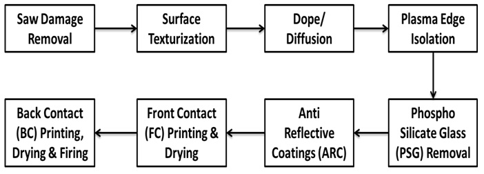
Figure 1: Conventional Process Flow of Silicon Solar Cell
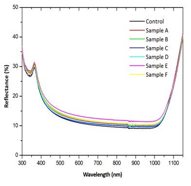
Figure 2: Total weighted reflectance of wafers processed with texture additive of different volumes at constant process time.
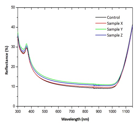
Figure 3: Total weighted reflectance of wafers processed with different process time.
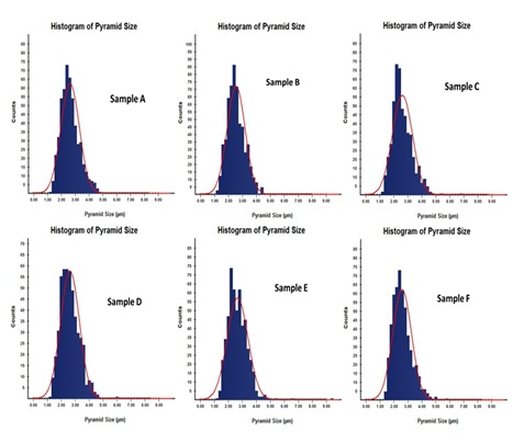
Figure 4: Pyramid Size of wafers processed with texture additive of different volumes at constant process time of 18 minutes.
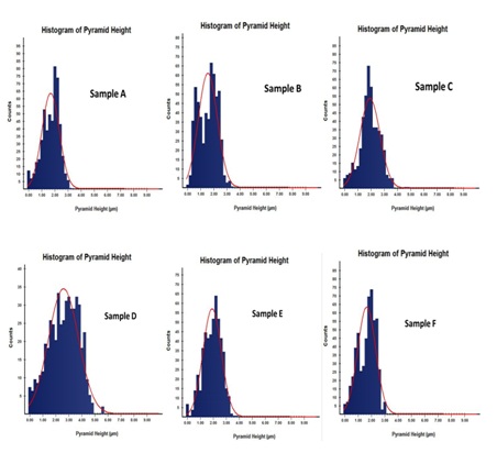
Figure 5: Pyramid height of wafers processed with texture additive of different volumes at constant process time
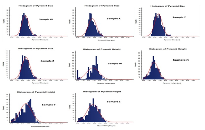
Figure 6: Pyramid size and height of wafers processed with 0.3% of texture-additive for different process times.
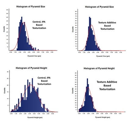
Figure 7: Pyramid size and height of wafers processed with and without texture additive (optimized)
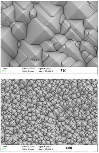
Figure 8: (a) Surface Morphology of wafers processed without texture additive, (b) Surface Morphology of wafers processed with texture additives (Optimized).
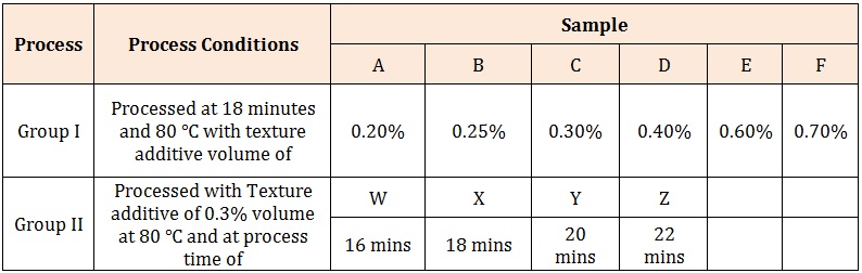
Table 1: Sample details with process conditions.
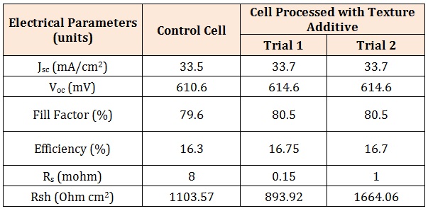
Table 2: Electrical Parameters of Cell with and without texture additive.