Role of Hydrogen in Films а-Si1-X Gex: H (X=0÷1) used as Solar Cells
Infrared (IR) absorption spectra are investigated hydrogenated amorphous solid solution films a-Si1-xGex: H (x = 0 ÷ 1) plasma chemical vapor deposition at different partial pressures of hydrogen PH2. Defined force, oscillator, which essentially depend on PH2. It is shown that the hydrogen contained in films mostly in the forms of GeH, SiH. Using integrated acquisitions JW, determined the amount of hydrogen in the films. Film properties depend on the composition and level of hydrogenation. The number of hydrogen atoms in films, varied by changing the composition of the gas mixture. In the work measured IR absorption for films a-Si1-xGex: H, a-Ge: H and a-Si0,88Ge0, 12: h. based on films and a-Si: H and a-Si0,88Ge0, 12: H fabricated three-layer solar cells with an area of item 1.3 cm2 and efficiency equal to ~ 9.5%.
Introduction
Introduction of Si Films and its alloy characterized by various structural phases. The most interesting of them are crystals that are in the amorphous matrix. Such alloys are produced by different methods at different technological regimes. For films of amorphous hydrogenated silicon and a-Si: H, formed by the method of cyclic sedimentation annealed in hydrogen plasma effect Stajeblera-Vronsky is expressed weakly [1]. Authors [2] note the absence of the effect of Stajeblera-Vronsky in Nanostructural films of a-Si: H film Silicon alloys crystallization of a-Si: H is carried out by various methods: long annealing in vacuum at 600°C, fast heat treatment [3], laser annealing [4] and ion implantation [5]. The mobility of the charge carriers, alloying and efficiency optical absorption coefficient in films of a-Si: Hvyshe than crystalline silicon. Films a-Si1-xGex: H are an effective and inexpensive material for making solar cells and other electronic devices [6, 7].
In this regard, the receipt of the aforementioned films and changing their conductivity type are actual tasks. Najafov BA, Fiqarov VR [8] shows that with the change in the temperature of the substrate grow Nano crystals increases. Found that with increasing concentration of average grain size decreases RN3 (d) and the proportion of crystalline particle volume (Vc). When alloying with increasing concentration of boron, B2H6, value (d) does not change, and Vc is reduced. The value of photo films and efficiency-Si1-xGex: H, somewhat lower than in a-Si: H [9, 10]. With the changing conditions of technology and technological parameters of hydrogen deposited on various structural phases: microcrystalline, polycrystalline, Nano crystalline, etc. of energy conversion efficiency based on Schottky barrier in films of a-Si: H was 5.5%. Attempts have been made to obtain high efficiency solar cell (CPAASE) (~ 9.0%) on the basis of a-Si1-xGex: H [11].
Most literature data show that when using amorphous silicon and Silicon-Germanium alloys in solar cells with multilayered or cascading structure have the greatest EFFICIENCY ~ 8.5% [12]. Based on the above stated the purpose of this work is to determine the amount of hydrogen in amorphous films method for optical solid solution a-Si1-xGex: H (x = 0-1) and manufacturing of solar cells based on them.
The Experimental Part
Thin films of a-Si1-xGex: H (x = 0-1) received plasma chemical deposition method using gas mixtures of H2 + SiH4, U + GeH4 in various proportions. Details on obtaining films shown in Nadjafov BA, Isakov GI, Abasov FP [11, 12]. Plasma RF field created through mainly inductive coupling. Film thickness was 0.1 ÷ 1.0 μm. Measured absorption coefficient (α), refraction (n), reflection (R), (T), width of band gap (E0) for each sample, using appropriate models [13, 14]. Optical absorption at room temperature were studied by the method of Timber VV, Solovvan MN, Najafov BA, Isakov GI [13, 14, 15, 16] on spectrometer x-29.
Results and Discussion
Hydrogen concentration in films а-Si1-xGex: H, (x=0÷1) determined by the method of Brodsky, et al [14, 15, 16, 17]:
( ) ANA N d αω
$$ r = \frac {A N _ {A}}{\left(\Gamma / \xi\right)} \int \frac {\alpha (\omega)}{\omega} d \omega $$ (1) ( ) Where N is the number of Avogadro and (ξ) the integral strength of the hydride with units cm2/mole (g/ξ) = 3.5. If the width of the absorption indicates through and center frequency ω * ω0, when ∆ ω/ω0 ≤ 0.1 after approximation with a tolerance of ± 2%, equation (1) can be written as follows:
( ) ANA N d αω
$$ = \frac {A N _ {A}}{\left(\Gamma / \xi\right) \omega_ {0}} \int \frac {\alpha (\omega)}{\omega} d \omega $$ (2) ( )
0
1 2 2 1 2 Where is: ( )
ε ε + = ; ε- dielectric constant. For Si,
2 9 A ε ε=12; Ge, ε =16. If the equation (2) integral expression Relabel АS and ( ) J d S $$ = \int_ {\omega_ {S}} \alpha (\omega) d \omega $$
–the cumulative uptake of fashion S stretching for each film, then in determining hydrogen concentration (NH) get a general expression in abbreviated form:
$$ N _ {H} = A _ {S} J _ {S} (3) $$
Coefficient АS–for films a-Si:H, is in the field of fashion stretching1,4∙1020 cm-2. Absorption coefficient (α) for these phones (2100 cm-1) is8∙10-1÷3∙102cm-1 When this NH=7∙1021÷2,1∙1022 cm-3. For films а-Ge:HАS =1,7∙1020 cm-2. In films a-Si:H and а-Ge:H absorption frequencies 2000 и 1980 сm-1 is caused by fluctuations in the type of valance and absorption frequencies 630 и 570 cm-1 oscillations of type bend (Figure 1a and 1 c).
α, cм -1
1980 a
830
| 630 830 | |
|---|---|
| 630 |
2200 2000 1800 800 600 ω, cм-1 Figure 1: Infrared absorption Spectra of amorphous films a-_Si:H (а), _a-_Si0,60Ge0,40:H (б) and a-Ge:H (в) $$ P _ {H _ {2}} = 3, 8 \mathrm {m T o r r}. $$ when Thus, forа-Si1-xGex: H the place has a significant overlap, which is observed in the spectrum of IR absorption for both bands stretching Ge: H (1980 cm-1) and Si: H(2000 cm-1), and for bending strips around the frequency600 сm-1 (Figure 1b) [5, 12]. It is clear that the equation (3), so did the links stretch fashion oscillating characterizes in films а-Si: H, а-Ge: Hиа-Si1-xGex:H. Assess the relative binding hydrogen to hydrogenated amorphous а_-Si1-xGex:H:
$$ = \left\{ \begin{array}{l} \frac {1}{I} \\ \end{array} \right. $$
$$ \frac {1}{r} \left\{\frac {x}{1 - x} \right. $$
N P x x N −
H Si (4)
1 − H Ge Where is NSi-H and NGe-H–hydrogen concentration in а-Si: H and а-Ge: H (вcm3). Equation (3) You can rewrite to fashion swings (wagging mode) films а-Si: H and а-Ge: H. Thus the value of the NSi-H and NGe-H are determined from equations (3) to fashion rocking in the following form:
$$ N _ {H} = A _ {W} J _ {W} (5) $$
where is, ( ) J d W w
αω $$ = \int_ {\omega_ {W}} \frac {\alpha (\omega)}{\omega} d \omega - $$
– the cumulative uptake of fashion swinging for films а-Si:H and а-Ge: H. For specified films Aw=1,6∙1019 cm-2 and Aw=1,1∙1019 сm-
3,accordingly. Knowing NGe-H (where, for films а-Ge: H, Aw=1,6∙1019 cm-2andα=5∙101 cm-1), calculate hydrogen concentration NH in the film_а_-Si1-xGex: H in the words of:
( ) •
α ω
1 ω ω ∫ d streets wag N N H Ge H
= − (6) ( ) α ω
2 ω ω ∫ d streets
Where is,
wag $$ N _ {G e - H} ^ {w a g} $$
– number of links Ge
H −
, some of the effects of net swing а-Ge: H, the value which, calculated according to the equation (5). The second factor in the expression for NH (cumulative ratio of IR absorption maxima) is a vibrational fashion stretching in the sample and in pure a-Ge: H. For the computation of the cumulative ratio used maximum satisfying the oscillatory fashion stretching Ge-H (2000 cm-1) in the film_а-Si1- xGex:H. From these data it is possible to evaluate the effect of the oscillator in filmа_-Si1-xGex:H the ratio of:
$$ \Gamma = J _ {S} / J _ {W} $$
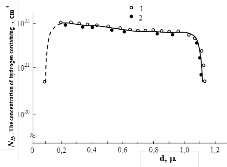
Where is, Ge Si J J J S S S ≈ + , Ge Si J J J W W W ≈ + . values , , , Ge Si Ge Si J J J J W W S S – are integrated acquisitions fashion, stretching and rocking, accordingly. The oscillator strength Г= 0,51 (for х=0) and Г=0,13 (for х=1). The maximum value Р=4,16 for х=0,40. Table 1 shows the characteristic parameters of amorphous films_а- Si0,60Ge0,40: H. On Figure 2 shows the distribution of hydrogen on film thickness d: certain1-method of recoil protons, 2-method of IR absorption spectrum. You can see, the distribution of hydrogen sufficiently uniform. Unlike other methods, the method of recoil protons (MOP) sample bombing beam of protons. When researching а_-Si:H and its alloys, this allows you to get distribution hydrogen on thickness~ 40 ÷ 100 Å. Method of calibration accuracy is limited only by theMCS, which is determined by the largest concentration of hydrogen(NH), and IR spectroscopy of found values that match 2 ÷ 3 %.
| № | E 0 | H | N Si:H | N Ge:H | N H | ||||||
|---|---|---|---|---|---|---|---|---|---|---|---|
| P mTorr H2 | P | I S(Si) | I S(Ge) | I W(Ge), I W(Si) | I /I S W | ||||||
| films | eV | at % | cm-3 | cm-3 | cm-3 | ||||||
| 1 | 0,6 | 1,32 | 1,85 | 1,3 | 6,2∙1021 | 2,2∙1021 | 3,1∙1020 | 7,2∙101 | 6,3∙101 | 6,0∙102 | 0,13 |
| 2 | 1,2 | 1,36 | 2,29 | 5,1 | 9,4∙1021 | 2,7∙1021 | 4,0∙1021 | 8,6∙101 | 7,5∙101 | 5,2∙102 | 0,18 |
| 3 | 1,8 | 1,41 | 2,59 | 8,7 | 1,3∙1022 | 3,3∙1021 | 5,1∙1021 | 9,4∙101 | 8,3∙101 | 4,0∙102 | 0,26 |
| 4 | 2,4 | 1,44 | 3,38 | 14,7 | 2,1∙1022 | 4,1∙1021 | 6,2∙1021 | 1,0∙102 | 9,0∙101 | 3,0∙102 | 0,38 |
| 5 | 3,0 | 1,52 | 4,16 | 23,7 | 2,9∙1022 | 4,6∙1021 | 9,7∙1021 | 1,1∙102 | 1,0∙102 | 2,7∙102 | 0,51 |
Table 2: Characteristic parameters of amorphous films a-Si0,60 Ge0,40: H.
This method provides information about the General content of both associated and not associated with Si hydrogen. А, with regard to the precise definition of hydrogen content in the volume of films, this band was analyzed INFRARED absorption 630 сm-1. To clarify the amount of hydrogen is embedded in amorphous matrix below as follows is determined by the structural parameter (R):
J R
2000 $$ ? = \frac {J _ {2 0 0 0}}{J _ {2 0 0 0} + J _ {2}} $$
+
2000 2100 Where is 2000 J and 2100 J – intensity of absorption bands at 2000 and 2100 cm-1. Using the equation (3), of this ratio is determined by the concentration of hydrogen. Increase R occurs simultaneously with a decrease in the concentration of hydrogen. The highest magnitude R (before 0,8) observed for films а-Si: H, the besieged plazmo chemical deposition method(ПХО), when TS=3000С, power frequency discharge W=100 Вт.
However, the films studied in the present work, that when TS=200 ÷ 3000С, microstructure parameter cannot vary in the range R= 0,1 ÷ 0,8. When annealing during 30 minutes in a vacuum at R value reaches 1.0. Accordingly, in this case, СH is 24.5 ÷ 14.0 at. %. By number of links Si- H, you can define a specific concentration of hydrogen containing links [Si–H]/[Si]. Specific concentrations of hydrogen containing Silicon links in the maximum reach the value 0.58 [10, 11, 12].
Hydrogen concentration (NH), some effusion method, correlated with the concentration of hydrogen, calculated using the integrated force IW, fashion rocking 600 cm-1 (Figure 3). The number of hydrogen atoms is found by aт % (СH), effusion method is defined for the data tapes and compared to the number of hydrogen atoms NА (Avogadro's number).
J A W W
Therefore, the ratio of
compared to СH (ат. %)
NH (Figure 3). Change СH (at. %) for films at various temperatures heat up, shown in the Table 1. Found that after effusion, during heat treatment up to 650° c, hydrogen concentration is NH=1,3 at %. In doing so, found that the strength of the oscillator depend Q on hydrogen concentration (NH), It decreases after effusion of hydrogen; with increased hydrogen content (РH2) in the atmosphere of the received films а-Si0,60Ge0,40:H When partial pressures from 0.6 to 3.0 mTorr power oscillator increases [5, 12]. This is due to the hydrogen containing links Ge:H, Si:H at specified frequency.
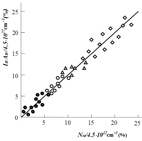
Figure 3: Correlation of concentrations of hydrogen effusion method defined by the integrated force IW, at a frequency of 600 cm-1, for the films a-_Si0,60Ge0,40:H. The films received at a pressure of hydrogen _PH2 = 0,6 мТорр. The films received at a pressure of hydrogen PH2 = 1,2 мТорр. The films received at a pressure of hydrogen PH2 = 1,8 мТорр.
= 2,4 The films received at a pressure of hydrogen PH2
мТорр.
= 3,0 The films received at a pressure of hydrogen PH2
мТорр.
Heating the sample in a closed volume is due to the fact that the material almost completely decomposed into its constituent elements, with crystallization temperature range 350 ÷ 6500С, What causes hydrogen jeffuziju and leads to increased pressure. Pressure measured capacitive pressure gauge with a precision of 0,1 %. To determine the effusion other gases should undertake quantitative mass spectrometric analysis of the composition of the gas.
Note that the hydrogen inside the film identifies several ways: at. %, NH, РH2 and Р. To define these settings, you must remove the IR absorption spectra of the corresponding frequency fluctuations associated with the absorption of hydrogen.
Optical Properties of Thin Films
The dependence of $(\alpha h v)^{1/2}$ from hv to determine the width of the forbidden zone [14, 16] for each film.
In all the studied films of the optical absorption edge ratio describes the ratio of:
$$\alpha h v = B \left( h v - E_0 \right)^2$$
(7)
where is, $\alpha = 5 \cdot 10^4 \text{cm}^{-1}$, $E_0$ - optical band gap width for each film, $B$ - the coefficient of proportionality. The value of the $B$ determined by extrapolation of dependencies $(\alpha h v)^{1/2}$ from hv for each sample. Quadratic dependence (7) received in theory model [13, 14], describes the density of States slit mobility. The value of the $B$ when $x=0 \div 1$ at. % Ge, for films $a$-Si1$_x$Gex: H changes from 527 before 343 eV$^{-1}$cm$^{1/2}$, accordingly, $E_0=1,86$ eV and $E_0=1,14$ eV. Means with increasing content of Germany, $E_0$ decreases. Mobility of carriers and photoconductivity in film $a$-Si1$_x$Gex: H, also diminishes when Germany more 40 ar. % [11, 12]. We use the known relative absorption coefficient $\alpha$ is determined from the following equation [14, 15, 16, 17]:
$$T = \frac{\left(1-R_1\right)\left(1-R_2\right)\left(1-R_3\right) \exp\left(-\alpha d\right)}{\left(1-R_2 R_3\right)\left\{1-\left[R_1 R_2+R_1 R_2\left(1-R_2\right)\right]^2\right\} \exp\left(-2\alpha d\right)}$$
(8)
Here take, that
$$R_1 = \left|(n-1)^2 + k_0^2\right| / \left|(n+1)^2 + k_0^2\right|$$
$$R_2 = \left|(n-n_1)^2 + k_0^2\right| / \left|(n+n_1)^2 + k_0^2\right|$$
$$R_3 = \left|(n_1-1)\right| / \left|(n_1+1)\right|^2$$
For weakly absorbing light areas $k_0^2 \leq (n-1,5)$. $k_0$ shows light attenuation in the substrate. Note that the film thickness $d$, defined in this case, the relevant transmission or reflection from extreme interference fringes.
From equation (8), the coefficients of absorption $(\alpha)$ are defined as follows:
$$T = \frac{kx}{a\left(1-bx\right)^2}$$
(10)
$$a T \left(1-bx\right)^2 = kx,$$
$$k \left(1-R_1\right)\left(1-R_2\right)\left(1-R_3\right),$$
$$a = 1-R_2 R_3,$$
$$b = R_1 R_2 + R_1 R_3\left(1-R_2\right)^3,$$
$$m = a T b, n = a T,$$
$$mx^2 + kx - n = 0.$$
Then,
$$\alpha = \frac{1}{d} \cdot \frac{2m}{k \pm \sqrt{k^2 + 4mn}}.$$
(11)
Equation (11) is a working formula for determining optical absorption coefficients for films, in a weakly absorbing spectral regions.
In a strongly absorbing spectral regions, $R_3 = 0, R_2 = R_1 = R$ and $n=n_1=1,5$ for glass substrates, a $n=n_1=3,42$ for silicon substrate. Then equation (8) can be rewritten as follows:
$$T = \frac{\left(1-R\right)^2 e^{-\alpha d}}{1-R^2 e^{-2\alpha d}};$$
$$x = e^{-\alpha d}; x^2 = e^{-2\alpha d}; T = \frac{\left(1-R\right)^2 x}{1-R^2 x^2};$$
Then,
$$p = \frac{\left(1-R\right)^2}{T}; \alpha = \frac{1}{d} \ln \left[ \frac{1}{2} \left(\sqrt{p^2 + 4R^2} + p\right) \right].$$
(13)
This formula can be used to determine the coefficient of optical absorption in a strongly absorbing spectral regions. Accordingly, the coefficients of refraction is defined using the following ratio:
$$nd = \frac{\lambda_m \lambda_{m-1}}{2\left(\lambda_{m-1} - \lambda_m\right)}$$
or the following formula:
$$\Delta n = \frac{c}{2\pi^2} \int \frac{\alpha(v)}{v^2} dv$$ (14)
Whereis $\lambda_m$, $\lambda_{m-1}$ – the wavelength corresponding to the
$$n(\lambda) = \left[ \frac{2n_1(T_{\max} - T_{\min})}{T_{\max} T_{\min}} + \frac{n_1^2 + 1}{2} \right] + \sqrt{\left( \frac{2n_1(T_{\max} - T_{\min})}{T_{\max} T_{\min}} + \frac{n_1^2 + 1}{2} \right)^2 - n_1^2} \frac{1}{2}$$
Whereis $T_{\max}$ and $T_{\min}$ – functions of the wavelength $\lambda$, $n_1$ – index of refraction of the substrate, which is defined by the expression:
$$n_1 = \frac{1}{T_1} - \sqrt{\frac{1}{T_1^2} - 1}$$
Whereis $T_1$ – deletion of the substrate, which is almost always in the area of transparency. As for glass substrates $T_1 = 0,91$, $\tau_{on} = 1,554$.
Accordingly, the film thickness is calculated by the formula:
$$d = \frac{A \lambda_1 \lambda_2}{2 \left[ n(\lambda_1 \lambda_2) - n(\lambda_2 \lambda_1) \right]}$$
Where is $\lambda_1$ and $\lambda_2$ – wavelengths which correspond to the neighbouring extreme points on the spectrum bandwidth, $A=1$ for two extremes of the same type (max–max, min–min) and $A=0,5$ for two adjacent extremums of the opposite type (max–min, min–max).
**Creation of Solar Cells**
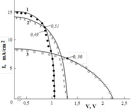
Studies show that films $a$-Si${1-x}$Ge$_x$H ($x \geq 0,20$) can be used as a qualitative material in semiconductor electronics [12]. For this purpose we have developed a 3-item based on two elements of cascade type. Three-layer element is made of 2-layer element consisting of two elements on the basis of $a$-Si: Hc $p$-i-$n$ transition and $p$-i-$n$ element with $i$-a layer of film $a$-Si${0.88}$Ge$_{0.12}$H. The thickness $i$-layers to the top two transitions selected in such a way that respected the condition of equality of short-circuit current lower element. Short circuit current was about half the value for an element with a $p$-i-$n$ transition. Idling voltage and short circuit current decreases with increasing number of superimposed layers. This way you can build multiple layers (create $n$-layer element). Note that for each item produced i-0.5 $\mu$m thick layer. The area of each element was 1.3 cm$^2$. When receiving a three-layer solar cells must be respected uniform thickness and square to each element. Substrate material of steel, and was chosen as the cover used ZrO$_2$ with missing light 80%. Covering the same time playing the role of upper ZrO$_2$ (front) of the contact. The thickness of the layers of $a$-Si: Hp and $n$-types was ~ 300 and 400$\mathring{\mathrm{A}}$, respectively. For alloying films number of B$_2$H$_6$ and PH$_3$ in gas mixtures changed within Alloy films in gas mixtures changed within 0.1 and 0.5%, respectively. After the deposition of amorphous semiconducting layers deposited by evaporation film ZrO$_2$ thickness ~ 500 $\mathring{\mathrm{A}}$. The upper contacts used Ni/Ag, for lower-stainless steel substrate. Items covered source sunlight provided AM-1 (100mVt/sm$^2$). Short-circuit current for 3-layer elements was 8,5mA/cm$^2$, no-load voltage ~ 2,25 V, fill factor ~ 0,50 and CPA ~ 9,5% (Figure 4). CPA for single-layer and double-layer element is 7% and 8.9%, respectively. The effectiveness of collecting media when different wavelengths is defined by the formula:
$$V(\lambda) = \frac{J_\Phi(\lambda)}{eN(\lambda)}$$ (15)
where is $J_\Phi(\lambda)$ – the photocurrent density (10 mA/cm$^2$), $N(\lambda)$ – the number of photons incident per unit surface per second, e-free media charge.
For elements with the structures of the short-circuit current is calculated in the supposition of a complete depletion of all layers, in the absence of direct bias. Thus, the short circuit current for the first, second, and third elements provides the following expressions:
( ) ( ) ( ) 1,24/ 03
$$ I _ {S c 3} = q \int_ {0} ^ {1, 2 4 / E _ {0 3}} (1 - R) N _ {p h} \exp \left(- 3 \alpha_ {n} W _ {n} - 2 \alpha_ {n} W _ {n} - 2 \alpha_ {p} W _ {p} - \alpha_ {1} W _ {1} - \alpha_ {2} W _ {2}\right) \left[ 1 - \exp \left(- \alpha_ {3} W _ {3}\right) \right] d \lambda \tag {16} $$
1 exp 3 2 2 1 exp 3 1 1 2 2 3 3 0
Where is, , , W W W n p i field distribution inside the , , i n p layer, respectively, N ph – the number of photons incident on the surface of the elements, R – reflectivity film, α –absorption coefficient for each layer elements. Idling voltage for cascading elements with two and three transitions is presented as:
$$ V _ {o c} (/ /) = 0, 5 \left(E _ {0 1} + E _ {0 2}\right) \tag {17} $$
$$ V _ {o c} \left(\mathrm {I I I}\right) = 0, 5 \left(E _ {0 1} + E _ {0 2} + E _ {0 3}\right) \tag {18} $$ The fill factor for all elements of the set size 0.5. Short- circuit current of a cascading element with two sets of values less transitions ( ) I II sc sets the lower value 1 sc I and 2 sc I . Short-circuit current of a cascading element with three passages is determined by the smallest amount of
1 sc I , 2 sc I или 3 sc I .
CPA of many transitional cascade elements is given by the expression:
( ) ( ) ( ) 0,5 0,5 0
$$ \eta (i) = 0, 5 \cdot 0, 5 \left(\sum_ {i} E _ {0 i}\right) \frac {I _ {s c} (i)}{P _ {i n}} \tag {19} $$ $$ W h e r e i s i = 2 $$
and 3 – shows the number of layers, Pin – power of incident light to the surface elements, its value is100 mV/cm2, , , 01 02 03 E E E – Accordingly, the width of the forbidden zone for each i -the layer. To raise η for solar cell, you want to increase the number of layers reduce the area elements, the choice of metal wires to reduce the resistance of the metal contacts, etc. Measurement of spectral sensitivity is usually produced at a constant illumination with white light, the intensity of which corresponds to the normal conditions of work (AM- 1~100 MVt/cm2), at the same time an element falls modulation calibrated monochromatic radiation. Photocurrent and its dependence on wavelength of monochromatic radiation is measured in shorted circuits by using synchronized amplifier. To determine the effectiveness of collecting important knowledge of the electric field which is passed to the element. It has been noticed that in device dependently to the configuration collection efficiency is offset from red light in the blue spectrum.
It is known that the photon energy and momentum of the corresponding electromagnetic wave with frequency and wavelength in vacuum, equal:
ν hc W hν $$ I = h \nu = \frac {h c}{\lambda}; P ^ {*} = \frac {h \nu}{c} = \frac {h}{\lambda}, $$ $$ = \frac {h \nu}{c} = \frac {h}{\lambda}, $$ c Where is, h- Planck's constant. When agile frequenciesν- the predominant role of wave properties, when large- particle properties of light. If the energy of electromagnetic radiation normally feed on some surface unit area for 1 sec, c-the speed of propagation of light waves in a vacuum, R-reflectivity surface pressure p-light on this surface is equal to:
$$ P = (1 + R) N \frac {h \nu}{c} = P ^ {*} / c (1 + R) [ 2 0 ] $$
* (1 ) / (1 ) h P R N P c R c
Light pressure (P) is defined by equation (20) and represent the following form:
* W hc N P
S S t λ = = (21)
N- the number of incident photons during $t$. W-photon energy falling at all wavelengths of the body surface. $P^*$ the momentum of the light falling on the dies surface 1 sec. Then the pressure of the incoming light is defined in the following form:
$$F = P \cdot S$$
$$F = \frac{hcNS(1+R)}{\lambda Stc} = \frac{hN(1+R)}{\lambda t}$$
$$F \lambda t = hN(1+R)$$
$$N = \frac{F \lambda t}{h(1+R)} \quad (22)$$
$F$ - the power of light pressure ($F=10^{-8}H$) on the surface ($S=1\text{cm}^2$), $\lambda$ - incident wave length, $t$ - time of incidence of the light for 1 sec. with energy $P^*$ and its value is Nhv - photons, and the momentum of each photon is equal to hv/c. With radiation reflection $R$ - and wavelength $\lambda$, the number of incident photons is $10^{17} \div 10^{18}m^{-2}c^{-1}$, $R = 0,2 \div 0,8$; $\lambda = 300 \div 900\text{ nm}$.
**Conclusion**
Thin films Obtained $a\text{-Si}_{1-x}\text{Ge}_x\text{H}$ ($x=0 \div 1$) plasma chemical deposition method using gas mixtures of $\text{H}_2 + \text{SiH}_4$; $\text{H}_2 + \text{GeH}_4$ in various proportions. It was determined that the highest R value (up to 0.8) is observed for films of $a\text{-Si}$. H deposited method (PCO) at temperature $t = 300^\circ\text{C}$, with an output frequency of discharge $W = 100\text{ W}$. The data on the ratio of
$$Q = \frac{I_S}{I_W}$$ the oscillator strength was assessed in the film $a\text{-Si}_{1-x}\text{Ge}_x\text{H}$. Where is $I_S = I_S^e + I_S^i; I_W = I_W^e + I_W^i$. The oscillator strength $Q=0,51$ (for $x=0$) and $Q=0,13$ (for $x=1$).
For $x=0,40$ the maximum value $P=4,16$.
Based on the films $a\text{-Si}$. H and $a\text{-Si}{0,88}\text{Ge}{0,12}$: H manufactured solar cells and created single-layer, double-layer and three-layer structure; their characteristics are measured. Found that for single-layer, double-layer and three-layer structures with an area element $1,3\text{cm}^2\eta$ is 7%; 8,9%; 9,5%, accordingly. For the three-layered element highs move in the scope of collection efficiency of longer wavelengths. In the reporting structures of their light in the wavelength interval $0,3 \div 1,1\text{ \mu}$, within 120 hours, there has been no degradation.
It is shown that the multi-layer structure solar cells based on $\text{Si}{10,88}\text{Ge}{0,12}$. H and $a\text{-Si}$. H and $a\text{-Si}$. H are effective, and the improvement of their EFFICIENCY are relevant tasks.
**References**
1. Wang Yan, Han Xiaoyan, Zhu Feng, HouGuofu, RenHuizhi (2006) Light induced degradation of microcrystalline silicon solar cells. J Non Cryst Solids 352(9-20): 1909-1912.
2. Shimazaki K, Imaizumi M (2007) JAEA 42(5).
3. Neretina S, Sochinskii NV, Mascher PJ (2006) Optical and microstructural characterization of the effects of rapid thermal annealing of CdTe thin films grown on Si (100) substrates. J Electron Mat 34(6): 786-790.
4. Stanimirova TJ, Atanasov PA, Stankova M, Stoyanchova TR, Dimitrova IG, et al. (2007) Optical and structural properties of undoped and palladium doped indium tin oxide films grown by pulsed laser deposition. J Appl Surface Sci 253(19): 8206-8209.
5. Chen Chao, Liu Yu-zhen, Zhang Cuo-bin (2007) J Luminescence 28(4): 579-584.
6. Matsui T, Ogata K, Isomura M, Kondo M (2006) Microcrystalline silicon–germanium alloys for solar cell application: Growth and material properties. J Non Crys Solids 352(9-20): 1255-1258.
7. Najafov BA (2016) Magazine fund research 7: 61-73.
8. Najafov BA, Fiqarov VR (2010) Hydrogen content evaluation in hydrogenated nanocrystalline silicon and its amorphous alloys with germanium and carbon. International Journal of Hydrogen Energy 35(9): 4361-4367.
9. Uchida Guchiro, Sato Muneharu, SeoHyunwoong (2013) Characteristics of photocurrent generation in the near-ultraviolet region in Si quantum-dot sensitized solar cells. Thin Solid Films 544: 93-98.
10. Sachenko AV, Korbutyak DV, Kryuchenko Yu, Kaganovich EB, Manoilov EG (2011) Photoelectric Properties of Heterostructures with Oxide Films Containing Si(Ge) Quantum Dots Formed by Pulsed Laser Deposition. Journal of Nanoelectronics and Optoelectronics 6(4): 420-426.
11. Nadjafov BA, Isakov GI (2007) Alternative energy and eco. 11: 177-178.
12. Najafov BA, Abasov FP (2015) Optoelectronic
processes of thin films and application prospects. LAP, Germany. с. 433.
13. Timber VV, Solovvan MN (2014) 56(10).
14. Najafov BA, Isakov GI (2005) 72(3): 371-376.
15. Najafov BA, Isakov GI (2010) Optical and electrical properties of amorphous Si1 − x C x : H films. 46(6): 624-630.
16. Najafov BA, Abasov FP (2014) Photonics Росc. 44(2):
72-90.
17. Najafov БА (2016) Int Journal of Applied and Basic
Research 12: 1613-1617.
References
-
Wang Yan, Han Xiaoyan, Zhu Feng, HouGuofu, RenHuizhi (2006) Light induced degradation of microcrystalline silicon solar cells. J Non Cryst Solids 352(9-20): 1909-1912.
-
Shimazaki K, Imaizumi M (2007) JAEA 42(5).
-
Neretina S, Sochinskii NV, Mascher PJ (2006) Optical and microstructural characterization of the effects of rapid thermal annealing of CdTe thin films grown on Si (100) substrates. J Electron Mat 34(6): 786-790.
-
Stanimirova TJ, Atanasov PA, Stankova M, Stoyanchova TR, Dimitrova IG, et al. (2007) Optical and structural properties of undoped and palladium doped indium tin oxide films grown by pulsed laser deposition. J Appl Surface Sci 253(19): 8206-8209.
-
Chen Chao, Liu Yu-zhen, Zhang Cuo-bin (2007) J Luminescence 28(4): 579-584.
-
Matsui T, Ogata K, Isomura M, Kondo M (2006) Microcrystalline silicon–germanium alloys for solar cell application: Growth and material properties. J Non Crys Solids 352(9-20): 1255-1258.
-
Najafov BA (2016) Magazine fund research 7: 61-73.
-
Najafov BA, Fiqarov VR (2010) Hydrogen content evaluation in hydrogenated nanocrystalline silicon and its amorphous alloys with germanium and carbon. International Journal of Hydrogen Energy 35(9): 4361-4367.
-
Uchida Guchiro, Sato Muneharu, SeoHyunwoong (2013) Characteristics of photocurrent generation in the near-ultraviolet region in Si quantum-dot sensitized solar cells. Thin Solid Films 544: 93-98.
-
Sachenko AV, Korbutyak DV, Kryuchenko Yu, Kaganovich EB, Manoilov EG (2011) Photoelectric Properties of Heterostructures with Oxide Films Containing Si(Ge) Quantum Dots Formed by Pulsed Laser Deposition. Journal of Nanoelectronics and Optoelectronics 6(4): 420-426.
-
Nadjafov BA, Isakov GI (2007) Alternative energy and eco. 11: 177-178.
-
Najafov BA, Abasov FP (2015) Optoelectronic processes of thin films and application prospects. LAP, Germany. с. 433.
-
Timber VV, Solovvan MN (2014) 56(10).
-
Najafov BA, Isakov GI (2005) 72(3): 371-376.
-
Najafov BA, Isakov GI (2010) Optical and electrical properties of amorphous Si1 − x C x : H films. 46(6): 624-630.
-
Najafov BA, Abasov FP (2014) Photonics Росc. 44(2): 72-90.
-
Najafov БА (2016) Int Journal of Applied and Basic Research 12: 1613-1617.
- Sense, Gravity, Parity & Chirality in Mathematical Physics
- Quantum Lattice Simulations PHYSICS: Microcircuit Particle Formation and Observable Macroscopic Irreversible Time - A Discrete Lagrangian with Cellular Automata Framework
- Quantum Biology from Biomacromolecule to Cell, and Central Dogma Described by Quantum Theory
- Focus, Agility, Speed and Technology (FAST) for Sustainability and Growth
- Square Root Metric Geometry and Pati-Salam Model in Curved Space-Time
- A Simple System Demonstrating the Mpemba Effect in Classical Mechanics