Effect of Thermal Nanocomposite NiO/C to Scale up the Absorption of Solar Energy on Flat Plate Collector
Novel coating consist of from nanoparticle NiO doped carbon thin film is explored with the optical and electrical properties was studied. This doping can help new excellent physical and chemical properties of carbon for photo-catalysis applications. Nanocomposite thin film was deposited on copper and glass substrates created by utilizing Spray Pyrolysis method. The precursor solution for the showering was blended Nanocomposite (NiO/C) with the polyethylene glycol as a colloidal. The SEM, UV, FTIR, XRD and AFM were used to check the behavior of the compositional components of the Nanocomposite and the energy gap of the Nanocomposite was computed. The reflection coefficient was determined from the measurements at room temperature in the wavelength range 400-1100 nm. Optical energy gap of Nanocomposite thin films have been estimated for the direct and indirect optical energy gap values determined and were 3.32 eV, 3.05 eV and photon energy 1.95 eV. The Nanocomposite activity under sunlight depends upon the band gap energy. Thin film of Nanocomposite NiO/C was sprained on the flat plate collector and then the useful energy was calculated from the solar energy before and after coating. The results demonstrated the coating on collector is very important to absorb solar energy that used to heat the water in domestic application. This paper has been achieved to dope carbon by nanoparticle of NiO for layer coating on flat plate collector. Results showed the efficiency of the collector increased (25%) by coating for Nanocomposite from absorption the solar energy light activity.
Introduction
Nanomaterials are attracted in enormous consideration in both principal studies and applications because of their novel physical and chemical properties to dope the particles of the material to product photo-catalytic forms. Real studies can possibly yield forward in most eminently in taking care of clean energy demand and handling natural contamination. The advancement of successful semiconductor photo- catalysts has raised into a standout objectives in materials science. A perfect photo-catalytic material would join the high action in regards to the applicable procedure of attention with high productivity of solar energy conversion. It ought Just a small amount of this energy is gathered by current photo-catalytic materials, which normally have a solar energy photo conversion. For a long time, the most inquired about the nanoparticles material is NiO; it has given the most proficient photo-catalytic action, highest stability, least cost and most minimal danger [1, 2]. Metal oxide NPs progress has numerous applications in solar energy conversion [3], superconductors [4] and absorbents. Metal-oxides constitute an essential class of materials that are associated with natural science; nickel oxide has pulled in much consideration as of late due to their significance both in science and innovation.
Uncommon consideration has been concentrated around the arrangement and properties of Nickel oxide (NiO), which is essential in particular, connected applications, for example, it has resistance for high-temperature [5, 6, 7], it has corrosive resistance. Its properties were controlled by their synthesis, structure, crystallinity, size, and morphology; incredible activities have been committed to the examination of various NiO materials combination [8]. It gives high surface zone and particular partiality for absorption in Nanocomposite.
The nanoparticles for NiO gives promising developments to compound, energy growth as a result of its strong of photo produced holes, while striking advances have been influenced, to address those troubles, recently, a broad thought has been focused around assembling particular NiO nanoparticles [9, 10]. Then NiO Nanoparticles have been made by various techniques including sol-gel, PVD, CVD, and co-precipitation [11].
These present attempts have revealed that doping carbon with NiO can achieve the progression of additional unmistakable dynamic impetuses. It is remarkable that metals have unique electronic properties, for example, examined its observable light activity for the regular blends [12]. On this line carbon doped by NiO nanoparticles organized to a raised temperature and unmistakably showed the capability of the NiO/C under solar light. Further, to produce a good absorption for this coating under solar light [13, 14].
The adequacy of photo activity depends upon high optical absorption [15, 16, 17, 18, 19]. The change proficiency of materials is managed by the band hole of the materials because of that the materials will permit all photons in the sun light with energies more important in the band gap. Most semiconductors have band gap and more holes. the empowered electron is moved into the conduction band of the semiconductor forsaking a hole limited from the valence band [20, 21].
Essentially, there are two sorts of optical band that can happen at the principal edge of crystalline semiconductors: direct or indirect advances. Both include the cooperation of an electromagnetic wave with an electron in the valence band, which is raised over the central hole to the conduction band. Nonetheless, the aberrant change likewise includes the concurrent connection with cross section vibration. Hence, the absorption coefficient α as a component of photon energy (Eg= hν) rely upon the energy of bands [22]. In this paper NiO/C, Nanocomposite were first integrated, and then obtained NiO/C to demonstrate obviously updated detectable light responding. These open entryways for the change photo-catalysis through carbon doped by nanomaterial, for instance, NiO and proposed instruments that showing the applications to begin a mix technique of the estimation of photo-catalytic activity. This paper considered nickel oxide (NiO) to doped carbon has been viewed as a remarkable semiconductor photo-catalyst as a result of its execution. Undoubtedly, photo-catalysis utilizing carbon doped by NiO to make another semiconductor for setting up another material that absorbed solar energy.
The value of the optical properties of the solar selective coating on the flat plate collector is very important to determine the heating of the water that pass through the collector from the solar energy and benefit from it in domestic applications for a good environment without contamination and minimal consumption for the of electricity
Experimental Details
Nanoparticle powder of NiO (99.9%, normal distance of 50 nm) and carbon (charcoal) have been set up from the market and working some procedure on it from: granulating and sieving to accomplish small scale molecule at that point taking SEM for the carbon molecule we find that the measurement of the molecule between (20.51-140.0 μm) was clarified in Figure 1.
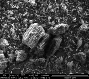
So using it as a coating material; then, the carbon powder gotten by a process after isolating it in a sieve (550 μm), then grindery the carbon and isolating it in the shifter (125 μm), later by SEM (Scanning Electronic Microscope) surveying the particle of the carbon and it find around (20.51-140.0 μm) shown in figure (1). After this stages, pounding the carbon and sieving it by a strainer (75 μm) and find the atom around (2.592-25.48 μm) this clarified in Figure 2.
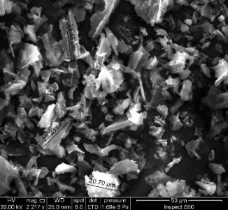
Figure 2: The SEM for the carbon (charcoal) in final stage. Besides, after complete grinding the carbon to get it powder, utilized to mix with NiO nanomaterial to doping carbon to estimate the photo-catalytic coating of the specimens. The Wt % of NiO with carbon was added to polyethylene glycol (PEG 400) to set up the colloidal before were the colloidal blended for (1 h) by a ultrasonic stirrer to ensure the mix up of a NiO/C Nanocomposite. The Nanocomposite scattered in (PEG 400) with add distilled water in the lab at room temperature, after that place it in the glass tube to start in coating the specimens by spray pyrolysis method. This equipment clarified in the Figure 3.
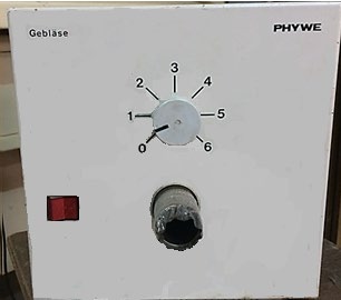
At that point, the air blower is utilized in the spray coating to blow the air under the activity of spray process, the blower equipment shown in Figure 4.
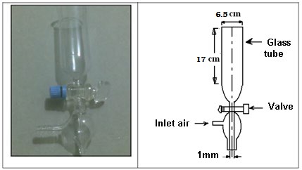
In the beginning of the spray procedure through the glass tube the colloidal pour from the hole in the top of the tube glass over, then will be showered on the samples through the glass tube. The glass chamber that envelops the capillary tube, this glass chamber at cone shape closes from the highest point of the valve that used to open and close the space of the capillary tube. The colloidal go down to the base of the substrate to splash through its. This glass chamber worked as a vacuum to show the effect inside the glass chamber to allow air to blend with colloidal beads in the end of a capillary tube to shower the colloidal on the samples. The air inters the side hole and meeting the beads of the colloidal toward the capillary tube to change the air pressure inside the glass cone. The spray cone shape implements on the samples that will be under the sprinkle space, the sample size was (2.5x2.5x0.2 cm3) was from the glass and (2.5x2.5x0.1 cm3) from copper as substrates. The sample puts under the atomizer, then putted underneath variation heater to enabling the sample to warming before begin in spray technique. The distilled water and PEG400 will vaporize under warming and samples will be dry. When completed the test; the dried samples puts in the furnace at temperature (250°C) for (6 h) to guarantee the crystallization of the Nanocomposite and leave them in the furnace to the next day when turning off the furnace. When the samples removed from the furnace the EDX and SEM estimations of the incorporated Nanocomposite were performed to affirm the carbon doping by NiO.
Catalyst Characterization
The specimens arranged by blended carbon and NiO Nano powder to be as a colloidal used in spray coating. The XRD diffraction equipment was SHIMATZU (CU-Kα1), radiation source (λ= 1.5406 Å) at 30 Kv and 20 mA, used to decide the compositions and precious crystal structures. The surface morphologies and cross-sectional microstructures of the examples were measured. The optical absorption spectra of the Nanocomposite were recorded utilizing SHIMATZU 1650 PC UV-VISIBLE spectrophotometer for the samples, with a wavelength range of 200–800 nm.
The FTIR spectrophotometer is a SHIMADZU FTIR-8300 FOURIER TRANSFORM INFRARED SPECTROMETER, it’s wavelength from (200-4000 cm-1) for spectral band width (2 cm-1).
Synthesis Semiconductor for Spectrally Selective Coatings (SSC)
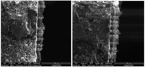
Approving a new design by utilizing NiO/C Nanocomposite as a semiconductor material that used as a coating for spectrally selective coatings (SSCs) on the surface of the flat plate collector. It is required to yield the light absorptivity in VIS–NIR extends because of the inherent band gap of Nanocomposite NiO/C (3.32 eV) for direct allowed transition and (3.05 eV) for indirect allowed transition. From the above experiment, the carbon doped by using nanoparticle in the covering is exceptionally advantageous for spectrally selective coatings (SSC) applications in a uniform spray covering. In Spray, covering process was utilized to deposit the NiO/C onto a cleaned copper substrate (Cu) surface and glass. The Nanocomposite (NiO/C) particles were scattered in (PEG 400), and blending to make a uniform colloidal. The Nanocomposite covered the substrates by spray pyrolysis. The film thickness was controlled from (45 to 160 μm) by modifying the shower covering conditions; this was inspected by SEM device. The film thickness compared by a great company, for example the ALMICO Company that analyzed its film thickness for covering by TiO2.
Results and Discussion
SEM Measurements for the Nanocomposite
The SEM picture shows Nanocomposite NiO/C as a semiconductor from tests, Figure 5 indicate Nanocomposite layer after coating on the samples. The nano particle NiO was scattered with various size of carbon as a coated layer on the samples. The thickness of the produced films was (45-160 μm) measured using SEM (Scanning Electronic Microscope: Inspect S50), where the thickness was produced films of NiO doped carbon when precipitated on glass films.
XRD Measurements for the Nanocomposite
The Nanocomposite NiO/C has been precipitated at room temperature on the samples and tested by utilizing X-ray diffraction equipment. The XRD demonstrates pinnacles of nanoparticles NiO and carbon before and after spray method for the samples are impressively expanded are appeared in table 1. This expansion of XRD test does not make any change, this prove that the Nanocomposite is a semiconductor because the position of the angles for the nano powder, carbon and the Nanocomposite are the same before and after the coating. This shown in Figure 6.
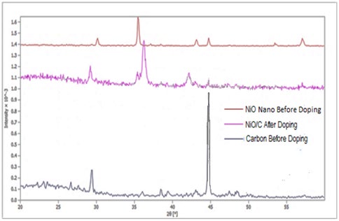
The Table 1 displays the crystalline size (D) in Angstrom, the crystalline size was calculated according to Debye- Scherrer formula and the diffraction heights consequently obtained from X-ray diffraction data that obtained from doping [23].
| No. | 2Theta (deg.) | D (Ao) | I/I1 | FWHM | Intensity (counts) |
|---|---|---|---|---|---|
| 1 | 29.22 | 3.05 | 27 | 0.342 | 71 |
| 2 | 36.25 | 2.48 | 100 | 0.456 | 260 |
| 3 | 42.13 | 2.14 | 28 | 0.476 | 73 |
| 4 | 44.7 | 2.03 | 5 | 0.288 | 13 |
| 5 | 53.6 | 1.71 | 5 | 0.221 | 12 |
| 6 | 57 | 1.61 | 3 | 0.3 | 15 |
Table 1: Peaks and the crystalline size of Nanocomposite NiO/C before and after doping.
The particle size was calculated using the Scherrer’s formula. The Scherrer formula is given by [24]:
$$ D = 0. 9 \lambda / \beta \cos \theta (1) $$
Where D is the normal molecule estimate opposite to the reflecting planes, (λ) is the X-ray wavelength, (β) is the full width at half maximum (FWHM), and (θ) is the diffraction point.
The Absorption coefficients (α), (Io) measured as the capacity of the energy of photon incident. Equation (2) depends on the Beer-Lambert law for optical absorption, (I) is the power of the transmitted light of the film with thickness (t), Absorbance (A), and the Absorption coefficient (α) which appeared in the accompanying condition [25]:
$$ \alpha = \frac {1}{t} * \ln \left(\frac {l o}{t}\right) = 2. 3 0 3 \frac {A}{t} $$ (2)
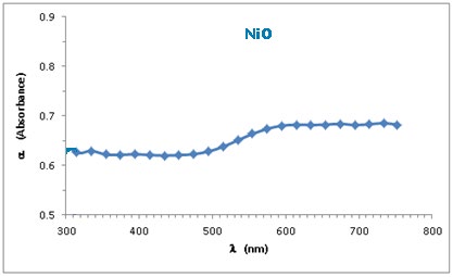
The absorbance versus wavelength follows for the sum of tests has been recorded in the range 200-800 nm as appeared in Figure 7.
Band Gap Energy Analysis for the Nano Composite
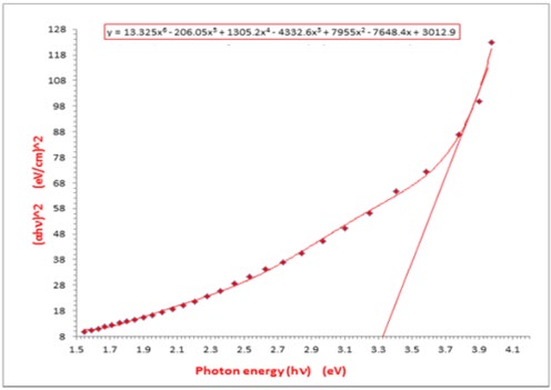
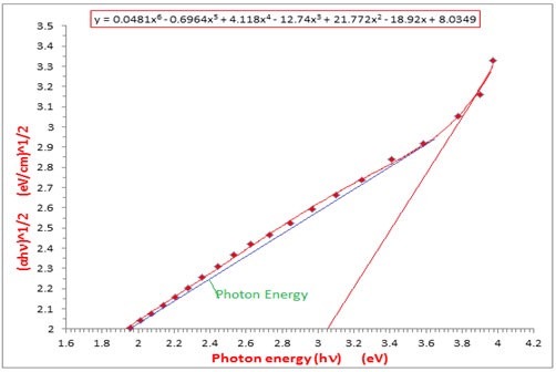
The absorption, which relates to electron excitation from the valence band to conduction band, can be utilized to decide the nature and estimation of the optical band gap. The connection between the absorption coefficients (α) and the incident photon energy (hν) can be composed as: The energy gap calculated from the optical band gap of the thin film for Nanocomposite NiO/C from the equation (3) [26, 27]:
$$ h v ^ {*} \alpha = A ^ {*} \left[ h v. E g \right] ^ {n} \tag {3} $$
Where (h) is the Planck constant (6.63 E-34), (ν) is the frequency (HZ (1/s)), Eg is the optical energy hole and A is exact consistent and exponent n relies upon the kind of progress. For direct allowed (n = 1/2), indirect allowed transition (n = 2).
The extrapolation of the straight line pivot gives the estimation of the energy band hole. At that point from the resultant of the NiO/C found that the direct allowed band gap estimations have been observed to be (3.32 eV) for direct transition, (3.05 eV) for indirect transition and the photon energy is (1.95 eV). At that point the outcome from the information of the results was shown in Table 2:
| Composite | Direct Allowed Transition | Indirect Allowed Transition | Photon Energy |
|---|---|---|---|
| C-NiO | 3.32 eV | 3.05 eV | 1.95 eV |
Table 2: the direct and indirect transition for the Nanocomposite NiO/C.
Then the Figures 8, 9 shows the result of the data for the direct, indirect transition and photon energy for a band gap to the Nanocomposite NiO/C.
The optical properties of the thin film for the Nanocomposite are measured in the wavelength from (200- 800 nm). The band gap is registered by the reflection UV- Vis spectra of NiO doped carbon appeared in figures 8 & 9 [28, 29].
The absorbance “α” is demonstrated for the band gap from the diagram, as the catch of the extrapolated straight piece of the plot. The capture comes at 3.32 eV so the band gap decided is 3.32 eV which have some sensible proportion. From the figures, the valence band happens at the point inverse of the conduction band is likewise on a similar point which displays that the (NiO/C) has a direct band gap.
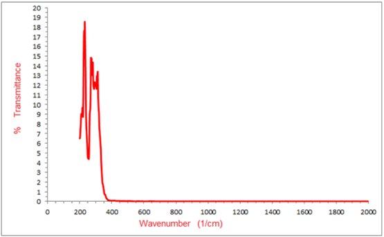
Transmittance Analysis for the Nanocomposite
The transmittance inspection for all samples for the Nanocomposite and inspected by the SHIMADZU equipment in UV-IR wavelengths, the resulting showed that there is no transmittance for the Nanocomposite for all samples during the tests. The Figure 10 showed the relationship drawn between the transmittance and the wavenumber for results test. The relation illustrates the transmittance start from the UV region as a 0.18 value and when it arrived at the visible region descended to zero value; this confirms that there is no transmittance in the Nanocomposite that utilized as a coating on the flat plate collectors and regard really as opaque materials. This Nanocomposite when precipitated on the substrate doesn’t permit the electromagnetic wavelengths as a solar energy to transmitted through it [30, 31].
FTIR Analysis for the Nanocomposite
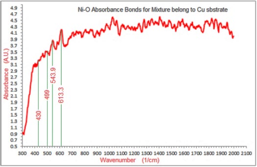
The covalent bonds in molecules are not rigid sticks or rods, which is found in molecular kits in the crystalline lattice for the compounds but likes stiff springs that can be stretched and bent. Virtually all the molecules for the chemical compounds will absorb infrared radiation that corresponds to energy to these vibrations. The absorption spectra obtained of compounds that are a unique reflection of their molecular structure in the crystalline lattice. The complication of infrared spectra between (200-1450 cm-
1); this region makes it difficult to assign all the absorption bands, more often called the fingerprint of the chemical structure of the material and be the strongest bands. The absorption bands in the region between (4000-1450 cm-1) are usually due to stretching vibrations of di-atomic units, and this is sometimes called the group frequency region, in the FTIR spectra broad band of Nanocomposite NiO/C that precipitates on the substrates. The peaks of Ni-O bonds stretching vibration appears in Figure 11 shows sharp absorption bands falls at regions (430, 499, 543.9 and 613.3 cm-1) respectively. In the present investigation, the observed peaks illustrated for Cr-O bond stretching vibration which be as a finger print of Nanocomposite NiO/C [32, 33].
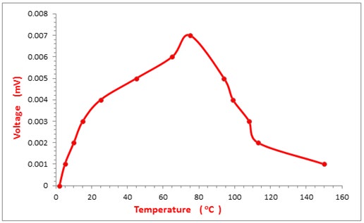
Seebeck Effect Analysis of the Nanocomposite
The Seebeck effect experiments found that if a piece of a Nanocomposite is connected to a voltmeter by two metal connections, and one side of the Nanocomposite is placed on the heated surface, and the other keeping in a cool surface then the galvanometer indicates that a current flows. From this thermoelectric effect was discovered during the experiment of the Nanocomposite, whilst the results of the experiment were proved for this Nanocomposite to be a semiconductor and the results exhibits a positive and negative resistance for each sample of Nanocomposite that precipitated on the substrates. Then the Seebeck effect only appeared when two dissimilar metals are connected as a Nanocomposite. It exhibit flow of the current causes by the resistance of the semiconductor can cause a reversible flow current through the junctions, and there is a temperature difference be determined across the semiconductor of the Nanocomposite recorded from the reading of the thermometers and the voltage difference reading by a voltmeter [34]. Figure 12 exhibits the Seebeck effect diagram for the Nanocomposite (NiO/C) explains the relation between the voltage difference and the temperature difference to gain the value of Seebeck effect and was between (20 to 6700 μV K-1), from the results of the Seebeck effect prove that the Nanocomposite (NiO/C) was a semiconductor synthesis by spray coating method.
Conclusion
Nanoparticle NiO utilized to doped carbon for photo- catalysts productivity; this created is solid and versatile for orchestrating NiO doped carbon for photo-catalyst. The Nanocomposite NiO/C show high noticeable light photo- catalytic action, this action is credited to the uniform NiO to doping carbon for precious crystals. The band gap value in the table considering the incredible photo-catalytic that created in an extensive variety of use in the solar energy. The experiments prove that the Nanocomposite was a semiconductor manufactured in this research and be a good coating in the flat plate collector to absorb the solar energy in excellent way without any transmittance or reflectance of the solar energy from the surface of the flat plate collector, because this coating will be a trap to the solar energy. Design and creation of this semiconductor structure for surface is based utilized as a part of spectrally selective coating (SSC). The Nanocomposite NiO/C is exceptionally for short-wavelength photons NIR and visible region for the semiconductor band gap. It found that the nanoparticle of NiO and bulk carbon particles have essentially improved the solar absorptivity compared with uniform nanoparticles because of the more productive light trapping. The results of the band gap exhibited a good agreement with the other researcher and there is no transmittance for the Nanocomposite. The FTIR analysis showed a good band stretching for the bond between the molecules of the Nanocomposite. The Seebeck effect analysis proved that the Nanocomposite was a semiconductor.
References
-
Fujishima A, Zhang X, Tryk DA (2008) TiO2 photocatalysis and related surface phenomena. Surf Sci Rep 63(12): 515-582.
-
Hashimoto K, Irie H, Fujishima A (2005) TiO2 photo- catalysis: a historical overview and future prospects. Jpn J Appl Phys 44(12): 8269-8285.
-
Xu JZ, Zhu JJ, Wang H, Chen HY (2003) Nano-sized copper oxide modified carbon paste electrodes as an amperometric sensor for amikacin. Analytical Letters 36(13): 2723-2733.
-
Pillai V, Kumar P, Hou MJ, Ayyub P, Shah DO (1995) Preparation of nanoparticles of silver halides, superconductors and magnetic materials using water- in-oil microemulsions as nano-reactors. Advance in colloid and Interface Science 55: 241-269.
-
Yang X, Peng X, Xu C, Wang F (2009) Electrochemical assembly of Ni–xCr–yAl nano composites with excellent high-temperature oxidation resistance. Journal of Electrochemical Society 156(5): C167-C175.
-
Jeffry IF, Ning L, Daniel D (1999) Spectral Tuning in the Human Blue Cone Pigment. Biochemistry 38(36): 11593-11596.
-
Rotter H, Landau MV, Carrera M, Goldfarb D, Herskowitz M (2004) High surface area chromia aerogel efficient catalyst and catalyst support for ethylacetate combustion. Applied Catalysis B 47(2): 111-126.
-
Chen L, Song Z, Wang X, Prikhodko SV, Hu J, et al. (2009) Three-dimensional morphology control during wet chemical synthesis of porous chromium oxide spheres. Appl Mater Interfaces 1: 1931-1937.
-
Chae WS, Lee SW, Kim YR (2005) Templating route to mesoporous nano crystalline titania nano fibers. Chem Mater 17: 3072-3074.
-
Jun YW, Casula MF, Sim JH, Kim SY, Cheon J (2003) Surfactant-Assisted Elimination of a High Energy Facet as a Means of Controlling the Shapes of TiO2 Nanocrystals. J Am Chem Soc 125: 15981-15985.
-
Zhang Z, Wang CC, Zakaria R, Ying JY (1998) Role of Particle Size in Nano crystalline TiO2-Based Photo- catalysts. J Phys Chem B 102: 10871-10878.
-
Kim S, Hwang SJ, Choi W (2005) Visible Light Active Platinum-Ion-Doped TiO2 Photocatalyst. J Phys Chem B 109: 24260-24267.
-
Choi Y, Umebayashi T, Yamamoto S, Tanaka S (2003) Fabrication of TiO2 photo-catalysts by oxidative annealing of TiC. J Mater Sci Lett 22: 1209-1211.
-
Wu Z, Dong F, Zhao W, Wang H, Liu Y, et. Al. (2009) The fabrication and characterization of novel carbon doped TiO2 nanotubes, nanowires and nanorods with high visible light photocatalytic activity. Nanotechnology 20(23): 235701-235710.
-
Bechstein R, Kitta M, Schutte J, Kuhnle A, Onishi H, et al. (2009) Evidence for Vacancy Creation by Chromium Doping of Rutile Titanium Dioxide (110). J Phys Chem C 113(8): 3277-3280.
-
Larsen GK, Fitzmorris R, Zhang JZ, Zhao Y, et al. (2011) Structural, Optical, and Photocatalytic Properties of Cr: TiO2 Nanorod Array Fabricated by Oblique Angle Co- deposition. J Phys Chem C 115: 16892-16903.
-
Bhosale R, Pujari S, Muley G, Pagare B, Gambhire A (2013) Visible-light-activated nano composite photo- catalyst of Cr2O3/SnO2. Journal of Nanostructure in Chemistry 3: 1-8.
-
Hajjaji A, Trabelsi K, Atyaoui A, Gaidi M, Bousselmi L, et al. (2014) Photocatalytic activity of Cr-doped TiO2 nanoparticles deposited on porous multi crystalline silicon films. Nanoscale Research Letters 9: 1-6.
-
Guan S, Hao L, Lu Y, Yoshida H, Asanuma H, et al. (2015) Fabrication of Photocatalyst Composite Coatings of Cr- TiO2 by Mechanical Coating Technique and Oxidation Process. Coatings 5(3): 545-556.
-
Yan H, Wang X, Yao M, Yao X (2013) Band structure design of semiconductors for enhanced photocatalytic activity: the case of TiO2. Progress in Natural Science: Materials International 23(4): 402-407.
-
Alamgir MK, Ansar MZ, Shoaib M, Murtaza G, Bhatti JA, et al. (2014) Tailoring the Energy Band Gap of Transition Metal Doped TiO2 Thin Film. Journal of Nano analysis 1(3): 129-134.
-
Eunah K, Zhong-Tao J, No K (2000) Measurement and Calculation of Optical Band Gap of Chromium Aluminum Oxide Films. Jpn J Appl Phys 39(8): 4820-4825.
-
Tabbal M, Kahwaji S, Christidis TC, Nsouli B, Zahraman K (2006) Pulsed laser deposition of nanostructured dichromium trioxide thin films. Thin Solid Films 515(4): 1976-1984.
-
Okolo B, Lamparter P, Welzel U, Mittemeijer EJ (2004) Stress, texture, and microstructure in niobium thin films sputter deposited onto amorphous substrates. J Appl Phys 95(2): 466.
-
Hamad TK (2013) Refractive Index Dispersion and Analysis of the Optical Parameters of (PMMA/PVA) Thin Film. Al-Nahrain Journal of Science 16(3): 164-170.
-
Ali A, Fadhil D, Yousif E, Hussain Z, Abdul-Wahab S (2017) A Comprehensive Study of Conductive Polymer Matrix Composites: A Review. Research Journal of Pharmaceutical, Biological and Chemical Sciences 8: 2043-2049.
-
Abed RN, Al-Sahib NK, Khalifa AJN (2017) Optical Study to Doping Carbon with TiO2 that Utilizing in Thermal Concentration. Oriental Journal of Physical Sciences 2: 109-113.
-
Julkarnain M, Hossain J, Sharif KS, Khan KA (2012) Optical properties of thermally evaporated Cr2O3 thin films. Canadian Journal on Chemical Engineering & Technology 3(4): 81-85.
-
Ivanova T, Gesheva K, Cziraki A, Szekeres A, Vlaikova E (2008) Structural transformations and their relation to the optoelectronic properties of chromium oxide thin films. Journal of Physics: Conference Series 113: 1-5.
-
Elwhab A, Alwany B, Samir OM, Algradee MA, Hafith MM, et al. (2015) Investigation of the Effect of Film Thickness and Heat Treatment on the Optical Properties of TeSeSn Thin Films. World Journal of Condensed Matter Physics 5(3): 220-231.
-
Ndegwa NG, Ndiritu FG, Hussein GSA, Kamweru PK, Kagia JK, et al. (2014) Reflectance, Transmittance and Absorptance of HDPE, LDPE, Glass and Sand Layer Used in a SAH. International Journal of Applied Physics and Mathematics 4(6): 406-4016.
-
Abdullah MM, Rajab FM, Al-Abbas SM (2014) Structural and optical characterization of Cr2O3 nanostructures: Evaluation of its dielectric properties. American Institute of Physics (AIP) advances 4(2): 1-11.
-
Diantoro M, Zaini MB, Muniroh Z, Nasikhudin, AHidayat (2017) The effect of Cr2O3 doping on structures and dielectric constants of SiO2-Bi2O3-B2O3-Na2CO3 glass based on silica gel of natural sand. International Conference on Physical Instrumentation and Advanced Materials. Journal of Physics Conf 853: 1-9.
-
Jenkins J, Jarvis WH, Ashhurst W (1971) Basic principles of electronics. Volume 2, Semiconductors, Elsevier, pp: 264.
- Sense, Gravity, Parity & Chirality in Mathematical Physics
- Quantum Lattice Simulations PHYSICS: Microcircuit Particle Formation and Observable Macroscopic Irreversible Time - A Discrete Lagrangian with Cellular Automata Framework
- Quantum Biology from Biomacromolecule to Cell, and Central Dogma Described by Quantum Theory
- Focus, Agility, Speed and Technology (FAST) for Sustainability and Growth
- Square Root Metric Geometry and Pati-Salam Model in Curved Space-Time
- A Simple System Demonstrating the Mpemba Effect in Classical Mechanics