Bright and Low Driving Voltage Top-Emitting Organic Light Emitting Diodes on Silicon
To match the driving voltage (3-5 V) of the driving circuits on silicon, we report an organic light-emitting device on silicon substrate featuring low turn-on voltage, high brightness. The fluorescent Alq3-based top-emitting organic light-emitting device with MoOx doped hole injecting layer shows a low turn-on voltage (voltage at the luminance of 1 cd/m2) of about 2.5 V and the brightness reaches 280 cd/m2 and 1400 cd/m2 at 4 V and 5 V, respectively. More importantly, we generated angular dependent electroluminescent spectra from the devices on silicon with narrow bandwidths which are crucial for encryption of visible light communication and may be useful for bio-light interaction.
Introduction
Organic light-emitting diodes (OLEDs) gained little attention until C. W. Tang fabricated the first low voltage and highly efficient OLED in 1987 [1]. From then on, OLEDs attracted great interests because of their superior performances, such as low cost, high efficiency, wide viewing-angle, fast response time and flexibility. In principle, an OLED consists of a sequence of organic layers between the anode and the cathode. Similar to the inorganic light-emitting diodes, the charge carriers drift through the injecting and transporting layers and meet in the emission layer under the positive bias. Subsequently, the excitons formed in the emitting layer decay radiatively to give light output. Meanwhile, a portion of the excitons would be quenched (decay non-radiatively), resulting in an energy loss. To date, OLEDs are considered to be the most promising alternative in displays (flat panel displays and flexible displays) and lighting. In terms of the driving scheme, OLED displays can be classified into two categories: passive matrix OLED (PMOLED) and active matrix OLED (AMOLED). As a new display technology, AMOLEDs are beneficial for the displays with high resolution and high information content, while PMOLEDs with simple structures are well suited for low cost and low information content applications. The active matrix driving mode, which implements a driving unit beneath each pixel, requires very complicated addressing circuits. This will drastically reduce the aperture ratio (AR) with bottom-emitting OLED (BEOLED) structures in which the emitting light travels through the substrates. Top-emitting OLED (TEOLED) structures have no such shortcoming as the light radiates in the opposite direction to the substrates. In addition to the owning of large AR, TEOLEDs can be integrated easily with any opaque substrate, such as silicon wafers and metallic foils. Recently, Paul Anthony Haigh et al. designed a visible light communication gadget with an OLED and an organic photodiode (OPD) and demonstrated high data transmission speed over 1Mb/s [2]. Claire M. Lochner et al. integrated green and red OLEDs with an OPD to construct a pulse oximeter which measured the pulse rate and oxygenation with very small errors [3]. Anja Steude et al. employed highly dense arrays of microscopic OLEDs as an optogenetic illumination platform to manipulate the behavior of living cells [4]. It is very encouraging and promising that OLEDs will play an important role in the communication and biomedical markets.
Purpose of this Work
The intrinsic organic charge injecting or/and transporting layers suffer from non-ideal injection and noticeable ohmic losses due to the large voltage drop outside the emitting layers (EML). For the intrinsic organic materials, the conductivities are relatively low, which lead to the inefficient charge injection from the electrodes into the organic materials. The OLEDs on the opaque substrates, which exploit highly dense electronic circuitries in a chip, e.g. silicon, are enabling a wave of portable and high information content products, such as heat-mounted displays for augment reality (AR) or virtual reality (VR), and micro/pico-projectors, a driving scheme without additional high voltage option is beneficial for low-cost mass production as the technology is compatible to the existing and mature complementary metal-oxide semiconductor (CMOS) driver technology. It’s our purpose to reduce the driving voltage and make the OLEDs integrated with a silicon circuit emit enough brightness. In response to this very specific demand, the concept of electrical doping is introduced [5], i.e. improving the injecting efficiencies of the carriers by doping the hole-injecting or transporting layer with p- dopants and/or doping the electron-injecting or transporting layer with n-dopants, and reducing the driving voltage. One of the most common p-dopants is 2,3,5,6-tetrafluoro-7,7,8,8-tetracyanoquinodimethane (F4-TCNQ) [6], and active metals, such as Cs and Li are usually used as n-dopants [5, 7, 8], which are usually not stable enough to handle and store in the ambient. Recently, transition metal oxides (TMOs), such as MoOx, V2O5 and WO3, are introduced as buffer layers [9, 10, 11] to improve the performances of the devices. In this letter, we fabricated bright and low-voltage TEOLEDs on silicon by doping MoOx into a hole-injecting layer 4,4′,4″,-tris(3- methylphenylphenylamino)triphenylamine (m-MTDATA). Similar to our previous report [12] in BEOLED, the p- doping layer greatly improved the properties of TEOLED. Here, we demonstrated a p-doped fluorescent device which showed a low turn-on voltage of about 2.5 V, and the driving voltages of 3.5 and 4.8 V respectively at a luminance of 100 and 1000 cd/m2 and small full-width-at- half-maxim a (FWHMs) of 37.6 and 37.4 nm, respectively.
Experiment
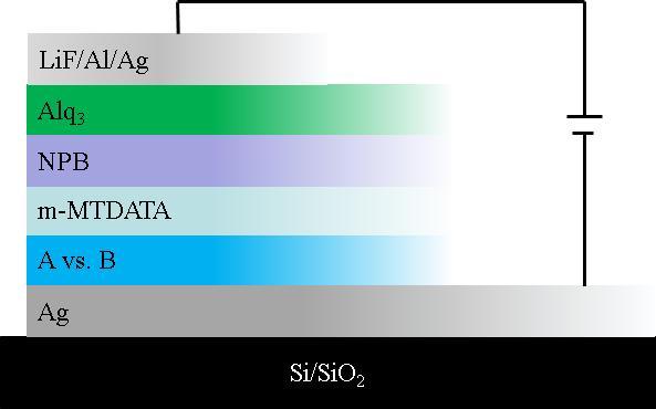
The anode with 70-nm-thick Ag film was deposited by vacuum evaporation onto a Si substrate covered with 340-nm-thick SiO2. After pumping the evaporation chamber down to a pressure of 10-4 Pa, 2 nm MoOx and 10 nm m-MTDATA and MoOx mixed layer with a doping ratio of 3:1 (molecule to molecule, m- MTDATA:MoOx=3:1) were deposited directly onto the Ag film for the devices A and B, respectively. The following layers were deposited by sequence. The structures (see Figure 1) were Si/SiO2/Ag (70 nm)/MoOx (2 nm)/m- MTDATA (45 nm)/NPB (5 nm)/Alq3 (60 nm)/LiF (1 nm)/Al (2 nm)/Ag (22 nm) and Si/SiO2/Ag (70 nm)/m- MTDATA:MoOx (3:1, 10 nm)/m-MTDATA (35 nm)/NPB (5 nm)/Alq3 (60 nm)/LiF (1 nm)/Al (2 nm)/Ag (22 nm) for the devices A and B, respectively. NPB, N, N′- bis(naphthalene-1-yl)-N,N′ –bis(phenyl)-benzidine, was used as the hole transporting layer (HTL), and Alq3, tris(8- hydroxy-quinoline) aluminum, served as the emitting layer (EML) and electron transporting layer (ETL). The organic materials were deposited at rates of 0.1- 1 Å/s and the metal contacts were at rates of 1-2 Å/s, respectively, monitored by the quartz crystal microbalances. The composite cathode, LiF/Al/Ag, was selected to simultaneously perform better electrical and optical properties. The electroluminescent (EL) spectra were measured by a PR650 spectrascan spectrometer. The luminance-current-voltage characteristics were recorded simultaneously by connecting the spectrometer with a source-meter-unit (Keithley 2400). The angular dependent EL spectra were collected by rotating the sample stage marked with the angle scale without shifting the spectrometer. The measurements were carried out in the ambient environments without encapsulating the devices.
Results and Discussion
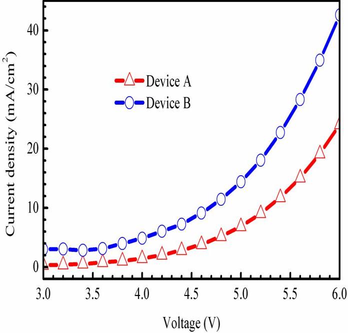
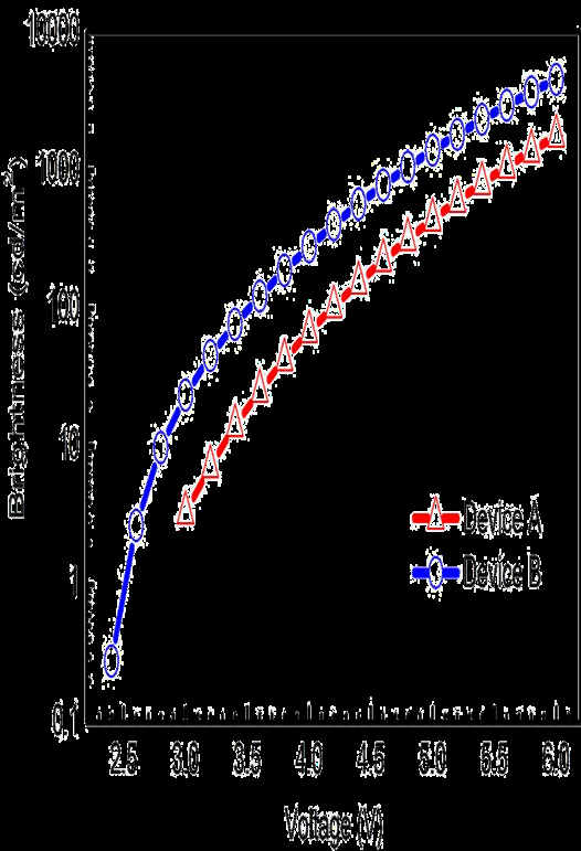
It’s demonstrated that the co-evaporation of MoOx and m-MTDATA leads to the formation of charge transfer complex in the mixed layer in our previous study [12]. The transferring of the electrons from m-MTDATA to MoOx causes a p-doping effect, (i.e. MoOx accepts electrons from the highest occupied molecular orbital (HOMO) of m-MTDATA to generate free holes.) which enhances the injection of holes from the anode and increases the conductivity in the bulk. (Figure 2) showed the current density-voltage characteristics of the devices A and B. It’s evident that the p-doped one (the device B) exhibited much higher current density due to its efficient hole injection. At the very low voltage, the current density of the device B is an order higher than that of the device A, while it’s approximately twice of that of the device A at the voltage above 5 V. As shown in (Figure 3), the device A with a MoOx buffer showed poorer brightness-voltage characteristics. The device B showed a low turn-on voltage of ~2.5 V and luminance of 100 and 1000 cd/m2 were achieved at 3.5 and 4.8 V, respectively, compared to 4.2 and 5.6 V of the device A. The maximum current efficiency of the device B, was improved by 40% attributed to the electrical doping.
It’s considered that holes have superior injecting ability to electrons in conventional OLED structures (without intentional the conductivity doping). The density of holes and electrons are quite out of balance. Why an improvement of the efficiency could be achieved in spite of the imbalance injection of holes and electrons from the electrodes? We attributed this property to the following ingredients. Firstly, the well modulated interfaces reduce the quenching of the emitters. As referred to our previous work [12], we found that the structure of NPB:MoOx/NPB/Alq3 would weaken the efficiencies of the device in spite of its superior hole injection to the non- doped one, while the structure of m-MTDATA:MoOx/m- MTDATA/NPB/Alq3 improved the performance of the device. We considered that the positive charges tended to accumulate at the interface of HIL/EBL (NPB was used both for HTL and EBL here. HIL is short for hole injecting layer and EBL for electron blocking layer.) for the latter structure, but not at the interface of EBL/EML. It’s considered that the excess holes at the interface of NPB/Alq3 will quench the excitons and lead to non- radiative recombination. Furthermore, the excess holes would be in favor of the formation of Alq3 cations, which is considered to be a major factor of the instability, aligned the energy level but also dissipated the accumulated holes at the interface of EBL/EML. This conclusion is consistent with the result of K. Leo’s group [5]. Secondly, the exciton recombination rate R is proportional to the product of the concentration of electrons and holes in the recombination region, i.e. R ∝ np, where n and p are the concentration of electrons and holes, respectively. As p increased, so did R when not saturated. Thus, the luminous efficiency would be improved. Finally, the p-doped HIL showing higher conductivity led to a reduction of the voltage dissipated outside the EML. The electrical doping reduces ohmic losses in the bulk of the injection or transport layers. It could help to reduce the additional joule heat and improve the stability. This doping also improves the probability of tunneling of holes from the anode due to the decrease of the thickness of the depletion region [2]. Due to the reduction of voltage dissipated outside the EML, an improvement of the electric field in the EML was achieved at the same bias compared with the one without electrical doping. It’s well known that μ∝ exp(αE1/2 ), where µ is the mobility of the carriers, α is the proportional constant, and E is the electric field [13]. It is deducible that the probability of the formation of electron-hole pairs and radiative recombination should be increased after the electrical doping, which leads to the improvement of the efficiencies.
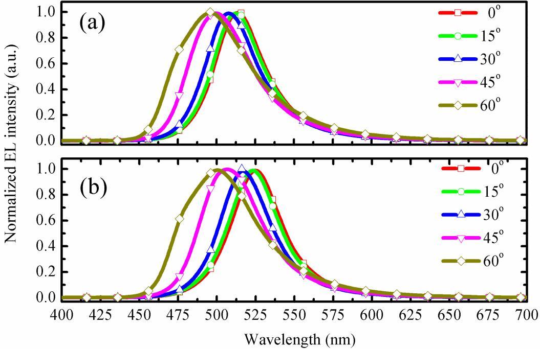
(Figures 4a and 4b) displays the angular dependent EL spectra of the TEOLEDs. It is known the OLEDs with the opaque and reflective bottom electrode exhibit strong microcavity effect. At the forward viewing angle, the devices A and B respectively show small FWHMs of 37.6 and 37.4 nm (see Table 1), and peaks at 512 and 524 nm, respectively. The drastic reduced FWHMs, compared to those of the counterpart BEOLEDs (~100 nm), render unique property for sensing and photodetection, e.g. usage in an oximeter and visible light communication, to decrease the background noise. The change of the EL peak wavelengths are mainly attributed to the variation of the refractive index of the hole transporting layer after doping MoOx. As the viewing angle increased, we observed gradually red-shifted EL peak wavelengths from 0 to 30o and then slightly regression of the peaks of both devices. This will be more useful for encryption in visible light communication as the EL spectra of a BEOLED is barely changed with the viewing angle and thus it is easier to be decoded.
| Device | Viewing angle (degree)/peak (nm) | ||||||||
|---|---|---|---|---|---|---|---|---|---|
| A | 0 | 15 | 30 | 45 | 60 | ||||
| FWHMa) | 37.6/512 | 37.7/512 | 39.5/508 | 46.8/500 | 56.8/496 | ||||
| B | 37.4/524 | 37.7/524 | 37.9/516 | 46.1/508 | 57.4/500 |
Table 1: Comparison of the FWHMs and EL peak wavelengths of the device
a)Full-width-at-half-maximum of the EL spectrum. Table 1: Comparison of the FWHMs and EL peak wavelengths of the device
Conclusions
In summary, we have demonstrated low driving voltage top-emitting organic light - emitting diodes with p-doping strategy for use in top emitting AMOLEDs, especially for OLEDs-on-silicon. The co-evaportion of MoOx and m-MTDATA leads to a charge transfer process, which releases excess free holes. The ohmic resistance of the injecting layer was reduced. The high-brightness TEOLEDs on silicon with high thermal conductivity shows promising application in visible light communication and biomedical treatment which require very highly intensive illumination sources with active matrix addressing. By introducing the cost-effective MoOx doping strategy, we are able to reduce ohmic loss and thus luminance loss of the OLEDs on opaque silicon substrates.
Acknowledgement
We gratefully acknowledge financial support from the National Natural Science Foundation of China (No.
61405069) and self-determined research funds of CCNU from the colleges¡¯ basic research and operation of MOE (CCNU15A02038).
References
-
Tang CW, VanSlyke SA (1987) Organic electroluminescent diodes. Appl Phy Lett 51(12): 913-915.
-
Paul AH, Zabih G, Ioannis P, Francesco A, Sandro FT, et al. ( 2013) IEEE Photonics Technology Letters 22: 2830-2833.
-
Claire ML, Yasser K, Adrien P, Ana CA (2014) Nature Communications 5: 5745-5751.
-
Anja Steude, Emily C Witts, Gareth B Miles, Malte C Gather (2016) Arrays of microscopic organic LEDs for high-resolution optogenetics. Science Advances 2(5).
-
Pfeiffer M, Leo K, Zhou X, Huang J S, Hofmann M, et al. (2003) Doped organic semiconductors: Physics and application in light emitting diodes. Organic Electronics 4(2-3): 89-103.
-
Gao W, Kahn A (2004) Controlled p-doping of zinc phthalocyanine by coevaporation with tetrafluorotetracyanoquinodimethane: A direct and inverse photoemission study. Appl Phys Lett 79: 4040-4042.
-
He G, Schneider O, Qin D, Zhou X, Pfeiffer M, et al. (2004) Very high-efficiency and low voltage phosphorescent organic light-emitting diodes based on a p-i-n junction. J Appl Phys 95: 5773-5777.
-
Huang J, Pfeiffer M, Werner A, Blochwitz J, Leo K, et al. (2002) Low-voltage organic electroluminescent devices using pin structures. Appl Phys Lett 80: 139- 141.
-
Cao J, Jiang X, Zhang Z (2006) MoOx modified Ag anode for top-emitting organic light-emitting devices. Appl Phys Lett 89: 252108.
-
Zhu XL, Sun JX, Peng HJ, Meng ZG, Wong M, et al. (2005) Vanadium pentoxide modified polycrystalline silicon anode for active-matrix organic light-emitting diodes. Appl Phys Lett 87: 153508.
-
Meyer J, Hamwi S, Bülow T, Johannes HH, Riedl T, et al. (2007) Highly efficient simplified organic light emitting diodes. Appl Phys Lett 91: 113506.
-
Xie G, Meng Y, Wu F, Tao C, Zhang D, et al. (2008) Very low turn-on voltage and high brightness tris-(8- hydroxyquinoline) aluminum-based organic light- emitting diodes with a MoOx pp-doping layer. Appl Phys Lett 92: 093305.
-
Gill WD (1972) Drift mobilities in amorphous charge- transfer complexes of trinitrofluorenone and poly-n- vinylcarbazole. Jour Appl Phys 43(12): 5033-5040.
- Solution-Processed Chiral Perovskites for Biomedical Applications
- Nanotechnology in Health Chemistry and Medicine: Current Challenges and Future Directions
- Human Exposure to Micro- and Nanoplastics: Pathways, Toxicity, and Intervention Strategies
- Exosome Nanomedicine for Cancer Therapy
- Micro and Nanoplastics–Plastisphere, Biotoxicity, Impact on Human Health, and Mitigation Strategies
- Process Validation of Cefixime Powder for Suspension Dosage Form, 50 mL