Optical Properties of Thin Films Alloy Si: H
In this work it is presented a methodology, based on optical properties, to determine the hydrogen concentration contained in films of a-Si: H and a-Ge: H. Moreover, it is shown that the film properties depend heavily on the composition and level of hydrogenation. The number of hydrogen atoms in the films were varied by changing trains and gas mixture measured infrared absorption for films of a-Si: H and a-Ge: H also defined width of forbidden zone E0 for these films. In the work of the IR absorption spectra are investigated alloy films and nk-Si: H (a-amorphous, nk-Nano crystalline) in the energy range 0.03 - 3.0 eV. Defined optical absorption coefficients (α) films for weakly and strongly absorbing spectra, as well as the coefficients of refraction (n) and weakening factors (active) for a variety of transparent and non-transparent substrates.
Introduction
In the world of science have been conducted adequate research in the direction of measurement and the study of thin films. However, in the direction of interference measurement and calculation of optical absorption has not received specific formulas that can help to simplify the analysis of the results of experimental work. In this work was carried out a brief analysis of the published numerous articles and it is presented some approaches that we consider can help to, improve the work of researchers. Thin films of Si and its alloys are is characterized by various structural phases. The most interesting of them are crystalline grains that are in an amorphous matrix. Effects of nana size of the thin films accompanied by formation of nanotubes, nanoparticles, Fullerenes, nana wire endofullerenes, graphites, grafans, clusters, etc. The formation of these nanomaterials is usually structural defects, presence and the role of hydrogen in their composition. Optical properties of nana- materials in the literature have been studied exhaustively.
Therefore, measurement of optical absorption coefficients (parameters (α), reflection (R), (T) transmission, refractive index (n) attenuation (active), thickness (d) of the thin films and their base the definition on the band gap (E0) for different applications [1, 2, 3, 4, 5, 6, 7, 8, 9, 10].
Results and Discussion
Consider the view of optical absorption edge of conductivity, for thin films:
$$ \mathrm {E} = \frac {1}{2} \mathrm {A} ^ {2} + \mathrm {B} ^ {2} $$
| N ( E )N (E ) | D |
|---|
$$ \mathrm {E} = \frac {1}{2} \mathrm {A} ^ {2} + \mathrm {B} ^ {2} $$
$$ \mathrm {E} = \mathrm {E} _ {1} + \mathrm {E} _ {2} + \dots + \mathrm {E} _ {n} $$ Where Ω is the sample volume and D is the matrix ∂ ∂ . For the appropriate ratio, get that matrix D for transitions between states of different zones and for transitions between not localized States is as follows:
element of the derivative operator x
$$ = \pi \left(\frac {a}{\Omega}\right) ^ {\frac {1}{2}} $$
a D π (1*) Where а is the average value of the interatomic distance. The value of D for localized wave functions, offset by a size multiplier between atomic distances rationing [1]. Therefore, for zone transitions are defined as:
2 2 2 8 ( ) ( ) ( ) 2 0
e a N E N E v c dE n cm π ω αω ω (2) where the integral shows the energy between the valence the zone and zone of conductivity. In the equation (2), $$ ) = \frac {8 \pi^ {2} e ^ {2} \hbar^ {2} a}{n _ {0} c m ^ {2}} \int \frac {N _ {v} (E) N _ {c} (E + \hbar)}{\hbar \omega} $$ $$ \mathrm {E} = \frac {1}{2} \mathrm {A} ^ {2} + \mathrm {B} ^ {2} $$ $$ \mathrm {E} = \frac {1}{2} \mathrm {A} ^ {2} + \mathrm {B} ^ {2} $$ $$ \mathrm {E} = \frac {1}{2} \mathrm {A} ^ {2} + \mathrm {B} ^ {2} $$
2 2 2 8 e a C const n cm π
$$ \mathrm {E} = \mathrm {E} _ {1} + \mathrm {E} _ {2} + \dots + \mathrm {E} _ {n} $$ = =
0 2 0 Moreover, let the density of states near the conduction band and around the valence band, it seems as:
s N E E E s c A
$$ ) = C _ {1} \left(E - E _ {A}\right) ^ {s}; 0 \leq s \leq 1 $$
( ) C ( ) ;0 1, 1
p N E E E p v B
$$ ) = C _ {2} \left(E _ {B} - E\right) ^ {p}; 0 \leq p \leq 1 $$
( ) C ( ) ;0 1, 2
s N E E E E c A ω ω
$$ ) = (E + \hbar \omega) = C _ {1} (E + \hbar \omega - I $$
( ) ( ) C ( ) 1
$$ \mathrm {E} = \frac {1}{2} \mathrm {A} ^ {2} + \mathrm {B} ^ {2} $$
(3) Based on the above ratios, equation (1) can be written in the following form:
p s E E E E B A C dE ω αω ω (4) Hence, we have that:
$$ ) = C _ {0} \int \frac {\mathrm {C} _ {2} \left(E _ {B} - E\right) ^ {P} \mathrm {C} _ {1} \left(E + \hbar \omega - B\right)}{\hbar \omega} $$ C ( ) C ( ) 2 1 ( ) 0 $$ \mathrm {E} = \mathrm {E} _ {1} + \mathrm {E} _ {2} + \dots + \mathrm {E} _ {n} $$ $$ \mathrm {E} = \frac {1}{2} \mathrm {A} ^ {2} + \mathrm {B} ^ {2} $$ C C 0 1 2 ( ) ( ) C ( ) 1 = − + − ∫ C p s E E E E dE B A αω ω ω (5) $$ v = \frac {E _ {A} - \hbar \omega - E}{E _ {A} - \hbar \omega - E _ {J}} $$ E E A y E E A B ω ω , and into account that it is possible to define E as:
$$ \mathrm {E} = \mathrm {E} _ {1} + \mathrm {E} _ {2} + \dots + \mathrm {E} _ {n} $$ $$ \mathrm {E} = \frac {1}{2} \mathrm {A} ^ {2} + \mathrm {B} ^ {2} $$ Now, let us to introduce the notation:
$$ \begin{array}{l} E = E _ {A} - E _ {B} \\ \mathrm {g e t :} \\ \end{array} $$
( ) ( ) 0 ω ω
$$ \left(- \hbar \omega\right) - E = \left(E _ {0} - \hbar\right) $$
E E E y A $$ \mathrm {E} = \frac {1}{2} \mathrm {A} ^ {2} + \mathrm {B} ^ {2} $$ ω ω $$ E = \left(E _ {0} - \hbar \omega\right) - \left(E _ {0} - \hbar\right) $$ ( ) ( ) , 0 0 E E E y $$ \mathrm {E} = \mathrm {E} _ {1} + \mathrm {E} _ {2} + \dots + \mathrm {E} _ {n} $$ ω ω $$ E = \left(E _ {A} - \hbar \omega\right) + (\hbar \omega - I $$ ( ) ( ) , 0 E E E y A $$ \mathrm {E} = \mathrm {E} _ {1} + \mathrm {E} _ {2} + \dots + \mathrm {E} _ {n} $$ ω = − ( ) . 0 dE E dy $$ \mathrm {E} = \mathrm {E} _ {1} + \mathrm {E} _ {2} + \dots + \mathrm {E} _ {n} $$ Moreover, by using the previous equations it is possible to get that:
$$ B - E = E _ {B} - E _ {A} + \hbar \omega - \left(\hbar \omega - E _ {0}\right) y = \left(\hbar \omega - E _ {0}\right) - \left(\hbar \omega - E _ {0}\right) y = \left(\hbar \omega - E _ {0}\right) (1 - y) $$ E E E E E y E E y E y B B A ω ω ω ω ω $$ \mathrm {E} = \mathrm {E} _ {1} + \mathrm {E} _ {2} + \dots + \mathrm {E} _ {n} $$ $$ E + \hbar \omega - E _ {A} = \left(E _ {A} - \hbar \omega\right) + \left(\hbar \omega - E _ {0}\right) y + \hbar \omega - E _ {A} = \left(\hbar \omega - E _ {0}\right) y $$ E E E E y E E y A A A ω ω ω ω ω $$ \mathrm {E} = \mathrm {E} _ {1} + \mathrm {E} _ {2} + \dots + \mathrm {E} _ {n} $$ Now, by substitution of equation (X) and (X) into equation (5) we can get: place the new equation in a new line and numbered it:
$$ \alpha (\omega) = \frac {C _ {0} C _ {1} C _ {2}}{\hbar \omega} \int (\hbar \omega - E _ {0}) ^ {p} (1 - y) ^ {p} (\hbar \omega - E _ {0}) y ^ {s} (\hbar \omega - E _ {0}) d y $$ $$ \mathrm {E} = \mathrm {E} _ {1} + \mathrm {E} _ {2} + \dots + \mathrm {E} _ {n} $$ $$ \mathrm {E} = \mathrm {E} _ {1} + \mathrm {E} _ {2} + \dots + \mathrm {E} _ {n} $$ or C C 0 1 2 1 ( ) (1 y) y ( ) 0 C p s s p E dy αω ω ω $$ ) = \frac {C _ {0} C _ {1} C _ {2}}{\hbar \omega} \int (1 - y) ^ {p} y ^ {s} \left(\hbar \omega - E _ {0}\right) ^ {s + p + 1} $$ $$ \mathrm {E} = \frac {1}{2} \mathrm {A} ^ {2} + \mathrm {B} ^ {2} $$ $$ \mathrm {E} = \mathrm {E} _ {1} + \mathrm {E} _ {2} + \dots + \mathrm {E} _ {n} $$ $$ \begin{array}{l} \int (1 - y) ^ {p} y ^ {s} \left(h \omega - E _ {0}\right) ^ {s + p + 1} d y \tag {7} \\ C _ {0} C _ {1} C _ {2} = \mathrm {c o n s t} \\ \end{array} $$ $$ ) = \operatorname {c o n s t} \int (1 - y) ^ {p} y ^ {s} \frac {\left(\hbar \omega - E _ {0}\right) ^ {s + p + 1}}{\hbar \omega} $$
1 ( ) 0 ( ) (1 y) y s p E p s const dy ω αω ω
$$ \mathrm {E} = \mathrm {E} _ {1} + \mathrm {E} _ {2} + \dots + \mathrm {E} _ {n} $$ $$ \mathrm {E} = \frac {1}{2} \mathrm {A} ^ {2} + \mathrm {B} ^ {2} $$ (8) For simplicity, you can write:
$$ ) = C _ {0} C _ {1} C _ {2} F (p, s) \frac {\left(\hbar \omega - E _ {0}\right) ^ {s + p + 1}}{\hbar \omega} $$
1 ( ) 0 ( ) C C ( , ) 0 1 2
s p E C F p s ω αω
$$ \mathrm {E} = \frac {1}{2} \mathrm {A} ^ {2} + \mathrm {B} ^ {2} $$
ω $$ \mathrm {E} = \mathrm {E} _ {1} + \mathrm {E} _ {2} + \dots + \mathrm {E} _ {n} $$ (9) $$ p = s = \frac {1}{2} $$ Now, if
2 ( ) 1 1 0 ( ) C C ( , ) 0 1 2 2 2
− = ω αω ω (10)
E C F $$ \mathrm {E} = \mathrm {E} _ {1} + \mathrm {E} _ {2} + \dots + \mathrm {E} _ {n} $$ $$ \mathrm {E} = \mathrm {E} _ {1} + \mathrm {E} _ {2} + \dots + \mathrm {E} _ {n} $$
1 1 C C ( , ) 0 1 2 2 2 C F const =
here So get that
$$\alpha(\omega) = \text{const} \frac{(\hbar \omega - E_0)^2}{\hbar \omega}$$
(11)
The results coincide with the formula found in formula found in literature data [1, 5].
Means for amorphous, nana crystalline films, forbidden zone width can be determined by using the equation (11). Note that the parameter $E_0$, in most films, describes the width of the forbidden zone.
Based on this model, we come to the conclusion that the tails of the valence band and conduction zones overlap. The donor and acceptor levels in these overlapping zones are associated with the same defects. In the area of overlapping conditions, position the Fermi level is constant. Another feature of the principle of this model is the existence of a "mobility" edges in the tails of the zones. These edges are identified with the previously entered mobility. Mott, critical energies that define localized State of non-localized, so this model is often referred to as model Motta-Cohen-Frice - Ovshinskows [1]. The difference between the energies of the edges in the mobility in the tails of the zones area of conduction and Valence zone indicates a width for the "forbidden zone for mobility" (slit for movement). Based on this model, it is assumed that the zone deep acceptors, partially filled with electrons created the weaker donor area. Donors and acceptors can change roles. Mott suggested that if these states arise from defect, for example, free connection, they can act as donors and as acceptors, and conditions of a single or double fill these conditions lead to the formation of two zones, separated by appropriate energy Hubbard.
Optical band gap width and other settings for the $a$-nk-Si:H and its alloys depend not only on the content of hydrogen, but also on other parameters, such as: substrate temperature, sedimentation rate, annealing temperature, composition, hydrogen partial pressure and the structure of the films. For amorphous and nana crystalline alloys (a-nk-Si: H), optical band gap determines the width of the data acquisition, which describes the ratio of (11). In this case equation (11) is as follows:
$$a \hbar \omega = B(\hbar \omega - E_0)^2$$
(12)
The value of the B for films $a$-Si$_{1-x}$Ge$_x$: H is $319 \div 547$ eV$^{-1}$ cm$^{-1/2}$
All films of the optical band gap width is described by the equation (12).
The hydrogen concentration in a-Si:H films is determined by the equation:
$$N = \frac{AN_A}{\Gamma/\xi} \int \frac{\alpha(\omega)}{\omega} d\omega$$
(13)
where, $N$ is Avogadro's number and ($\Gamma/\xi$) is the integral force of the hydride with the unit of measurement cm$^2$/mol, ($\Gamma/\xi$) = 3.5. Let us denote the spectral width as is denoted by $\Delta\omega$ and the center of frequency as $\omega 0$, and then at $\Delta\omega / \omega 0 \leq 0.1$, after approximation with an error of $\pm 2\%,$ equation (14) can be written in the following form [2, 3, 4, 5, 6, 7, 8, 9, 10]:
$$N = \frac{AN_A}{\Gamma/\xi} \omega_0 \int \frac{\alpha(\omega)}{\omega} d\omega$$
(14)
where, $\varepsilon$ is the dielectric constant. For Si, $\varepsilon = 12$; Ge $\varepsilon = 16$.
Accordingly here:
$$T = \frac{(1-R_1)(1-R_2)(1-R_3) \exp(-\alpha d)}{(1-R_2 R_3) \left\{ 1 - \left[ R_1 R_2 + R_1 R_3 (1-R_2) \right]^2 \exp(-2\alpha d) \right\}}$$
and
$$R_1 = \left| (n-1)^2 + k_0^2 \right| / \left| (n+1)^2 + k_0^2 \right|$$
$$R_2 = \left| (n-n_1)^2 + k_0^2 \right| / \left| (n+n_1)^2 + k_0^2 \right|$$
$$R_3 = \left| (n_1-1) \right| / \left| (n_1+1) \right|^2$$
For weakly absorbing light areas $k_0^2 \leq (n-1,5)$. Active shows weakening of light in the system of film-substrate. Note that the film thickness $d$, defined in this case, the relevant transmission or reflection from extreme interference fringes.
Accordingly, the thickness of films in all cases and circumstances is calculated from equation (17), if $n$- is the refraction coefficient is known. Note that for glass and silicon substrates $n$ equals 1.5 and 3.42, respectively.
$$d = \frac{K \lambda_1 \lambda_2}{2 \left[ n(\lambda_1 \lambda_2) - n(\lambda_2 \lambda_1) \right]}$$
(17)
where λ1 и λ2 -wavelengths which correspond to the neighboring extreme points on the spectrum band width, K = 1 for two extremes of the same type (max-max, min- min) and K = 0.5 to two neighboring extremes opposite type (max-min, min-max).
This equation is in good agreement with the equation for the transparent substrate in strongly and weakly absorbing spectral regions. In here R1, R2, R3 accordingly, the reflection of the light-air film, film-substrate, the substrate-air. α- absorption coefficient of the films, d- film thickness, T- light transmission, n-refractive index and active-factor weakening of light in the film-substrate system, 1 n - the coefficients of refraction of the substrate. From equation (16):
( )2 2 1 0 − +
n k $$ \frac {n - 1) ^ {-} + k _ {0} ^ {2}}{n + 1) ^ {2} + k _ {0} ^ {2}} = 1 $$ R n k 2 4 ( 1) 2 2 1 ( 1) 0 1 1 1 1
1 2 2 ( 1) 0
R n n k n R R 2 2 ( ) 1 0
$$ = \frac {4 n - (n + 1) ^ {2}}{1 - R _ {1}} + \frac {R _ {1}}{1 - R _ {1}} (n + 1 $$ − + n n k $$ \frac {\mathrm {i} - n _ {1}) ^ {2} + k _ {0} ^ {2}}{\mathrm {i} - n _ {1}) ^ {2} + k _ {0} ^ {2}} = I $$ R n n k 2 2 ( ) 1 0 1 1 2 2 2 ( ) 1 0
2 2 2 ( ) 1 0
$$ 1 - R _ {2} = 1 - \frac {\left(n - n _ {1}\right) ^ {2} + k}{\left(n + n _ {1}\right) ^ {2} + k} $$ n n k R + + n n k 2 4 ( ) 2 1 1 2 ( ) 0 1 1 1 2 2 $$ = \sqrt {\frac {4 n n _ {1} - \left(n + n _ {1}\right) ^ {2}}{1 - R _ {2}} + \frac {R _ {2}}{1 - R _ {2}} (n + n)} $$ nn n n R k n n R R (18) Equation (18) is determined by the coefficient of attenuation (active) in the alloy films а-nк-Si: Н. Consider special cases: 1) n=1 then:
$$ R _ {1} = \frac {k _ {0} ^ {2}}{4 + k _ {0} ^ {2}} $$
k R + k
1 1 1 ( 1) 2 4 1 0
| 1 2 | 1 1 R 1 |
|---|
| 2 | R 1 |
|---|---|
| 1R 1 |
$$ \frac {1}{k _ {0} ^ {2}} = \frac {1}{4} \left(\frac {1}{R _ {1}} - 1\right) $$ , , , $$ = R _ {2} = \frac {(n - 1) ^ {2} + k}{(n + 1) ^ {2}} $$ n k R R + + n k When 1 2 R R R = = , then 0 3 R =
2 2 ( 1) 0 2 2 ( 1) 0
− + n k $$ \begin{array}{l} \frac {+ k _ {0} ^ {2}}{+ k _ {0} ^ {2}} = R k _ {0} ^ {2} = \frac {4 n - (n + 1) ^ {2}}{1 - R} + \frac {R}{1 + R} (n + 1) ^ {2} \\ k _ {0} ^ {2} = \frac {1}{1 - R} \left[ 4 n - (n + 1) ^ {2} + R (n + 1) ^ {2} \right] \\ \end{array} $$ $$ \frac {\mathrm {i} - 1) ^ {2} + k _ {0} ^ {2}}{\mathrm {i} + 1) ^ {2} + k _ {0} ^ {2}} = 1 $$ R n k , = − + + + − k n n R n R 2) If n=1, then:
2 2 (1 ) 1 0 2 2 2 (1 ) 1 0
$$ = \frac {\left(1 - n _ {1}\right) ^ {2} + h}{\left(1 + n _ {1}\right) ^ {2} + h} $$ n k R + + n k 2 2 ( 1) 1 0 − + n k $$ \frac {- 1) ^ {2} + k _ {0} ^ {2}}{+ 1) ^ {2} + k _ {0} ^ {2}} = 1 $$ R n k 1 2 2 2 4 ( 1) ( 1) 0 1 1 2 1 1 2
2 2 2 ( 1) 1 0
$$ k _ {0} ^ {2} = \frac {1}{1 - R _ {2}} \left[ 4 n _ {1} - \left(n _ {1} + 1\right) ^ {2} - R _ {2} \left(n _ {1} + 1\right) ^ {2} \right] $$
3)
If n1=1, then
$$ \begin{array}{l} \text {I f n} _ {1} = 1, \text {t h e n} R _ {3} = 0: \\ \frac {(1 - R _ {1}) (1 - R _ {2}) \exp (- \alpha d)}{1 - R _ {1} R _ {2} \exp (- 2 \alpha d)} \tag {19} \\ \end{array} $$ $$ \gamma = \frac {\left(1 - R _ {1}\right) \left(1 - R _ {2}\right) \exp (- \alpha)}{1 - R _ {1} R _ {2} \exp (- 2 \alpha d)} $$ α R R d T R R d α (19)
2 (1 ) exp( ) 2 1 exp( 2 )
$$ Y = \frac {(1 - R) ^ {2} \exp (- \alpha)}{1 - R ^ {2} \exp (- 2 \alpha)} $$
α R d T $$ \text {i f} R _ {1} = R _ {2} = I $$
R , then:
− − α (20) 2 (1 ) exp( )
R d $$ T = \frac {(1 - R) ^ {2} \exp (- \alpha)}{\Gamma} $$
α R d T
2 1 exp( ) − −
α R d (1 )(1 ) exp( )
α $$ \prime = \frac {(1 - R) (1 - R) \exp (- a)}{\left[ \right]} $$
R R d T − − + − (21) 2 2 ( 1) 0 2 2 ( 1) 0
α α
1 exp( ) 1 exp( )
R d R d $$ 1 = \frac {(n - 1) ^ {2} + k}{(n + 1) ^ {2} + k} $$
n k R + + n k 4) n=1 and n1=1, then:
$$ R _ {1} = R _ {2} = R = \frac {k _ {0} ^ {2}}{4 + k _ {0} ^ {2}} $$
k R R R + $$ \begin{array}{l} - K _ {2} - K - \frac {1}{4 + k _ {0} ^ {2}}, \\ 1 - R = \frac {4}{4 + k _ {0} ^ {2}}, \\ \end{array} $$ + R k , 4 2 ( ) exp( ) 2 4 0 2 $$ r = \frac {\left(\frac {4}{4 + k _ {0} ^ {2}}\right) ^ {2} \exp (- a)}{k ^ {2}} $$ α d k T k
2 0 1 ( ) exp( 2 ) 2 4 0
− − + α d k
, − = α
16exp( ) 2 2 4 (4 ) exp( 2 ) 0 0
d T + − α , 16exp( ) 2 4 4 16 2 exp( 2 ) 0 0 0
k k d − = α
d T + + − −
α , k k k d
$$ \cdot = \frac {1 6 \exp (- \alpha d)}{\left[ 4 + k _ {0} ^ {2} - k _ {0} ^ {2} \exp (- \alpha d) \right] \left[ 4 + k _ {0} ^ {2} + k _ {0} ^ {2} \exp (- \alpha d) \right]} $$ α
16exp( ) 2 2 2 2 4 exp( ) 4 exp( ) 0 0 0 0
d T α α k k d k k d
and $$ \begin{array}{l} \left. k _ {0} - k _ {0} \exp (- \alpha a) \right] \left[ 4 + k _ {0} + k _ {0} \exp (- \alpha a) \right], \\ \exp (- \alpha d) = y, \\ y = \frac {1 6 y}{(4 + k _ {0} ^ {2} - k _ {0} ^ {2} y) (4 + k _ {0} ^ {2} + k _ {0} ^ {2} y)}, \\ \end{array} $$ y T + − + + $$ \begin{array}{l} + k _ {0} ^ {2} - k _ {0} ^ {2} y) \left(4 + k _ {0} ^ {2} + k _ {0} ^ {2} y\right), \\ = \frac {1 6 y}{\left(4 + k _ {0} ^ {2}\right) ^ {2} - k _ {0} ^ {4} y ^ {2}}, \\ \end{array} $$ y T + −
| 8 T | 64 2 2 (4k ) 2 0 T |
|---|
k , 2 2 2 64 (4 ) 8 0 4 4 0 0
$$ v = \frac {8}{T _ {k} ^ {4}} \pm \frac {\sqrt {6 4 - (4 + k)}}{T _ {k} ^ {4}} $$ k T y $$ \begin{array}{l} T k _ {0} ^ {4} ^ {\perp} T k _ {0} ^ {4} \\ \exp (- \alpha d) = y \\ \end{array} $$ $$ \alpha d = \ln \frac {1}{y} $$ $$ - \alpha d = \ln y, ^ {\alpha} $$ =
| 8 | 2 2 2 64(4k ) T 0 |
|---|
$$ = \frac {8}{4 + k _ {0} ^ {2}} $$
+ T $$ \alpha d = \ln \frac {T}{8} k _ {0} ^ {4}, $$
k и , $$ ! = \ln \frac {k _ {0} ^ {4}}{4 + k _ {0} ^ {2}} $$
k d $$ l = \ln \frac {1}{8} T k _ {0} ^ {4} = \ln \frac {1}{8} \frac {8}{4 + k _ {0} ^ {2}} $$ k α k α + d Tk + ,
2 (4 ) 8 0 + k T , then:
| 8 | D |
|---|
In here:
Tk
| 8 | D |
|---|
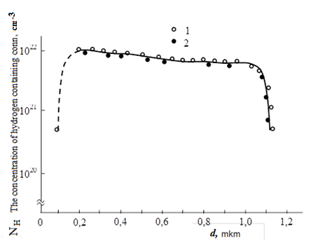
Table 1 shows the characteristic parameters of amorphous films. On the Figure 1 shows the distribution of hydrogen on film thickness (d): certain 1-method recoil protons, 2-method of IR absorption spectrum. It can be seen that the distribution of hydrogen sufficiently uniform. Note that values of NH, some method of recoil protons (MRP) and IR spectroscopy match 2-3 at. %.
The concentration of hydrogen (NH), a certain method of effusion, correlated with the concentration of hydrogen, calculated using the integrated force IW, at a frequency of 600 cm-1 swing fashion (Figure 2).
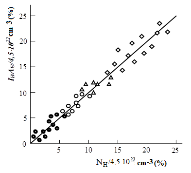
-films obtained by hydrogen pressure 0.6 mTorr. -the film received when hydrogen pressure 1.2 mTorr. -the film received when hydrogen pressure 1.8 mTorr. -the film received at a pressure of hydrogen 2.4 mTorr. -the film received when hydrogen pressure 3.0 mTorr.
Conclusion
One of the main objectives of this article is to facilitate the work of researchers engaged in semiconductor physics experimenter’s thin films. The results provide an opportunity to determine the optical band gap width, the coefficients of light transmission, reflection, refraction, optical absorption, as well as to determine the thickness of films during the deposition. The results also give an opportunity to conduct experiments spectrometer ICS-21, ICS-14A, ICS-22, ICS-29, FT - IR spectrometer Varian 640 JR, who work in the field of wavelengths 0,75-45 μm.
| E 0 | H | N Si:H | N Ge:H | N H | |||||||
|---|---|---|---|---|---|---|---|---|---|---|---|
| № film | P H2 mTorr | P | I (Si) S | I (Ge) S | I (Ge), I (Si) W W | I /I S W | |||||
| eV | at % | sm-3 | sm-3 | sm-3 | |||||||
| 1 | 0,6 | 1,32 | 1,85 | 1,3 | 6,2∙1021 | 2,2∙1021 | 3,1∙1020 | 7,2∙101 | 6,3∙101 | 6,0∙102 | 0,13 |
| 2 | 1,2 | 1,36 | 2,29 | 5,1 | 9,4∙1021 | 2,7∙1021 | 4,0∙1021 | 8,6∙101 | 7,5∙101 | 5,2∙102 | 0,18 |
| 3 | 1,8 | 1,41 | 2,59 | 8,7 | 1,3∙1022 | 3,3∙1021 | 5,1∙1021 | 9,4∙101 | 8,3∙101 | 4,0∙102 | 0,26 |
| 4 | 2,4 | 1,44 | 3,38 | 14,7 | 2,1∙1022 | 4,1∙1021 | 6,2∙1021 | 1,0∙102 | 9,0∙101 | 3,0∙102 | 0,38 |
| 5 | 3,0 | 1,52 | 4,16 | 23,7 | 2,9∙1022 | 4,6∙1021 | 9,7∙1021 | 1,1∙102 | 1,0∙102 | 2,7∙102 | 0,51 |
References
-
Davis EA, Mott NF (1970) Conduction in non- crystalline systems V. Conductivity, optical absorption and photoconductivity in amorphous semiconductors. Phil Mag 22(179): 903-922.
-
Najafov B (2017) Spectrophotometric analysis of thin film alloys a-nkSi: H. Germany, Lambert, pp: 80.
-
Najafov B (2010) Hydrogen content evaluation in hydrogenated nano crystalline silicon and its amorphous alloys with germanium and carbon. International Journal of Hydrogen Energy 35(9): 4361-4367.
-
Najafov BA, Isakov GI (2007) ISJAEE. 11: 177-178.
-
Najafov BA, Abasov FP (2015) Optoelectronic thin film processes and prospects of application. LAP, pp: 433.
-
Shimazaki K, Imaizumi M (2007) Japan Atomic Energy Agency. 42: 5.
-
Najafov BA, Isakov GI (2005) Layer-by-Layer Laser Spectrum Microanalysis of Easel-Painting Materials. Journal of Applied Spectroscopy 72(3): 371-375.
-
Najafov BA, Isakov GI (2010) Optical and electrical properties of amorphous Si1 − x C x: H films. Inorganic materials 46(6): 624-630.
-
Najafov BA, Abasov FP (2014) Photonics Ross 44(2): 72-90.
-
Najafov BA (2016) Int Journal of Applied and Fundamental Research 12: 1613-1617.
- Sense, Gravity, Parity & Chirality in Mathematical Physics
- Quantum Lattice Simulations PHYSICS: Microcircuit Particle Formation and Observable Macroscopic Irreversible Time - A Discrete Lagrangian with Cellular Automata Framework
- Quantum Biology from Biomacromolecule to Cell, and Central Dogma Described by Quantum Theory
- Focus, Agility, Speed and Technology (FAST) for Sustainability and Growth
- Square Root Metric Geometry and Pati-Salam Model in Curved Space-Time
- A Simple System Demonstrating the Mpemba Effect in Classical Mechanics