Photoelectric Properties of Nano Composite Material Films TiO2/SnO2 Prepared by Co-Spraying Pyrolysis Method
Mixed films TiO2/SnO2 were prepared by co-pyrolysis method from solution mixture of TiCl4 and SnCl4 salts. Investigating results of X-ray diffraction showed that upon spray pyrolysis conditions were carried out, compounds of TiCl4 and SnCl4 are not affected each other. Thus, oxide material systems were created from pyrolysis TiCl4 and SnCl4 salts which are the mixed systems of nano composite shape. Special point of these films is that there are appearances of photoconductivity that depends strongly on ratio of initial materials and prepared temperatures. Absorptive spectrum UV – Vis and luminescent spectrum of nano composite (nco) TiO2/SnO2 films were measured to determine width of forbidden band. Results showed absorption and luminescent spectrum of them all have red moving to visible light region, these showed that there is narrowing forbidden band of nco TiO2/SnO2 films compared with nano TiO2 films prepared by the same method. The electric properties of the films as surface’s resistivity, carrier density, sensitivity of carriers based on Hall Effect were also carried out to explain for role of component phases within changing photo-electric properties of nano TiO2 films.
Introduction
TiO2 is wide band gap semiconductor (3,2 eV), thus on usual condition it almost has not free carriers in conductive band, it will be excited when it is illuminated by ultra violet (UV) radiation which has wave-length of less than 388 nm. However, nano TiO2 films still do not conduct electricity when illuminated it by UV radiation. This is by in wide band gap semiconductor system with nano particle structure, they have tendency to create high energy potential fence on grain boundary, prevent transfer of the excited electrons between particles. Therefore, there is no photoconductivity current passing pattern under effect of external electric field. These characteristics have limited applying potential of the material in reality including in both photocatalysis and photoelectric fields. To enhance the use of value of nano TiO2 material, one of research directions which has been selecting on the world is mixing suitable impurities into material [1, 2, 3], or preparing multi-component materials based on nano TiO2 [4, 5, 6, 7, 8]. These types of materials at once can be excited by ultraviolet radiations (UV) or visible range of lights (Vis) and have electric conductive potential in normal conditions. These allow to enhance photoelectric efficiency and expand applying range on areas of photocatalysis, solar cell, UV sensor and photoelectric applications. In this work, we studied a few photoelectric properties of TiO2/SnO2 nano composite material films prepared by co-spraying pyrolysis from solution mixture of salts TiCl4 and SnCl4.
Experiments
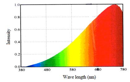
Photoconductivity spectrum or photoresistance spectrum of prepared films were carried out by resistant measurement when film was illuminated by the light passing monocolour spectrometer CARL ZEISS-JENA. Excited radiation illuminate pattern used light of halogen lamp 12 V – 50 W has radiation spectrum show on (Figure 1). Electric parameters of the prepared films were defined based on Hall effect and carried out on device Hall Lakershore MODEL 665, U.S.A. Combining measurements of Hall effect and conductivity (resistance) of semiconductor may determine carriers concentration, sort of carrier and Hall sensitivity H = RH (RH – Hall constant). Between Hall sensitivity H and swept sensitivity has relation: ratio H/ typical change in range 1 - 2 dependence on predominating scattering mechanisms, namely depended on temperature and concentration of impurities.
UV-Vis absorption spectra were measured by the Shimadzu UV-Vis 2540 absorptive spectrometer. In near ultraviolet, visible and near Infra-red ranges, semiconductors strongly absorb electro-magnetic radiations (depended on width of band gap Eg) by mechanism creating electron-hole couples in photon energy larger than width of band gap (basic absorptive edge). Thus, measurement on basic absorptive edge helps to determine Eg of semiconductor easily. Luminescent spectra were measured by the fluorescence spectroscopy FL 3-22 Jobin – Yvon – Spec., USA. From energy peak of luminescent spectra may receive information about width of band gap and energy levels of electrons, alloy components, the binding energy of the alloy (and the exciton), the tension inside and width of the quantum wells. X-ray diffraction patterns (XRD) of films were measured by the D8-AVANCE BRUKER X-ray diffractometer using Cu Kα radiation (k = 0.1542nm) with scan rate of 0.02°/sec. TiCl4 99% of Meck (Germany). SnCl4.5H2O 99% of Chinese production.
Results and Discussion
Survey pyrolysis regulations of SnCl4
To implement technologies to create composite films TiO2/SnO2, must first determine the SnCl4 pyrolysis mode - the material used to make transparent electrode films conductivity. Substrate temperature is the most important element of the SnO2 film formation process as it relates directly to the thermodynamics of chemical decomposition process SnCl4. SnO2. Resistance of the film is first important parameters need to be examined. SnO2 film was prepared by spray pyrolysis method from SnCl4.5H2O solution with concentration of 0.125 M. In order to intensify the film conductivity, the initial solution is doped with a small amount of NH4F + HF mixture (3.5%). Figure 2 shows the dependence of surface resistivity of the film versus the substrate temperature. Thermodynamics of chemical decomposition process SnCl4 to form SnO2 film dependence on pyrolysis temperature, it is related to the crystallinity, the amount of impurities and oxygen blank nodes in SnO2 lattice formation, and thus related to the resistance (conductivity) of the film. The results showed that the optimal temperature regime to prepare SnO2 material by spray pyrolysis method SnCl4 solution is in the range of 380 – 410°C. In this temperature region, the most legitimate film formation, concentration and largest mobility of electrons [9]; surface resistance of the film reaches a value below 10/□. This result is consistent with the results of the authors [10, 11].
Survey of composite material systems TiO2 and SnO2 manufactured by co-pyrolysis method
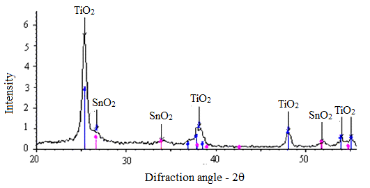
Initial solution is a mixture of TiCl4 (0.1 M) and SnCl4 (0.1 M). The concentration ratio of the components in the mixture varies from 100% of SnCl4 to 100% of TiCl4. Substrate temperature is varied from 390 to 450°C, that is temperature range to form TiO2 and SnO2 compounds from pyrolysis reaction of TiCl4 and SnCl4 salts respectively. The interaction of the two materials is assessed through the identifying phase components by XRD. Results showed that, with all the mixing ratios, the XRD of patterns contain the only diffraction peak of TiO2 and SnO2, there was no expression of the diffraction peaks of other phases formed simultaneously contains Ti, Sn, O. This proves that in the pyrolysis conditions carried out here TiCl4 and SnCl4 compounds do not interact with each other. Such oxide material systems formed from pyrolysis of salt is a composite mixture, containing simultaneously two types of oxide and is denoted TiO2/SnO2. Survey photoconductive properties of TiO2/SnO2 film: XRD schema of TiO2/SnO2, which prepared with 7% mol SnCl4 at 425°C substrate temperature is shown in Figure 3. It was found that the film contains primarily of anatase TiO2 with small amounts is SnO2 exist separately.
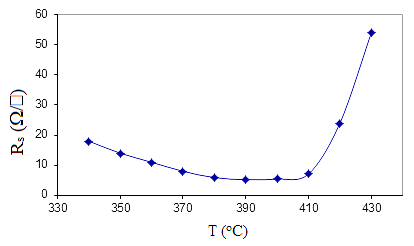
Figure 3: Schematic of the X-ray diffraction pattern with the mol ratio of 7% SnCl4 substrates prepared at temperatures of 425°C. I-V characteristic of the transition between the TiO2/SnO2 and SnO2 electrode was prepared is shown in Figure 4. The results show that it is in contact Ohmic. The particular found in this film is appearance of photoconductive properties depend strongly on the initial rate of materials and prepared temperature. To examine this characteristic, the film is made as photoresistor with electrodes SnO2: F prepared by spray pyrolysis method.
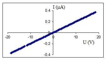
Figure 4: Volt-Ampere characteristic of SnO2-TiO2/SnO2 contact. The light resistance RL of films is measured in the light of a halogen lamp 12 V - 50 W at the distance of 10 cm. Survey results on prepared temperature is given in Table 1. From these results it can be seen that temperatures corresponding with the largest photosensitivity is about 425°C.
| 350 | 375 | 400 | 425 | 450 | |
| $R_{D(K) | 3200 | 2900 | 2400 | 16500 | 20000 |
| R_{L(K) | 1400 | 620 | 320 | 45 | 200 |
| R_{D/RL}$ | 2.3 | 4.7 | 16.9 | 337 | 100 |
Table 1: Characteristics of TiO2/SnO2 photoresistor depends on the substrate temperature TS.
| 2 | 4 | 6 | 8 | 10 | |
| Rt(K) | 24000 | 21000 | 20000 | 16000 | 2100 |
| Rs(K) | 4900 | 45 | 16.4 | 14.5 | 8.5 |
| Rt/Rs | 4.9 | 467 | 1220 | 1103 | 247 |
Table 2: Characteristics of the photoresistor film TiO2/SnO2 in substrate temperature of 425°C with different ratios of SnCl4.
Table 2: Characteristics of the photoresistor film TiO2/SnO2 in substrate temperature of 425°C with different ratios of SnCl4. When SnCl4 concentrations in the initial mixture are low, SnO2 were formed and the adsorbed onto boundary of TiO2 particles are little and dispersed, they reduce potential barrier between TiO2 particle boundaries but not much. So Rs of film is large and ratio RD/RL is small. When SnCl4 concentration increases, the forming SnO2 adsorbed onto boundary of nanoparticles TiO2 increased, numerously decreased potential barrier on boundary of nanoparticles, photoexcited electrons of TiO2 easily shift between the particles under the influence of external fields, ratio RD/RL increases. Conversely, at higher concentrations of SnCl4, formedSnO2 phase linked together to form an electric conducted network, reduced photoelectric effect and led to decrease in RD/RL ratios. Thus, depending on the composition ratio of SnO2 in the film, with the dual role of SnO2 both effect of reducing boundary potential barrier of TiO2 nanoparticles, both effect of forming conductive phase. So having the optimum region of SnCl4 rate led to maximum RD/RL ratios.
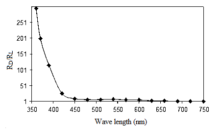
Pyrolysis process of SnCl4 solution led to the formation of SnO2 phase with high conductivity, resistance of SnO2 depended on pyrolysis temperature and had the minimum value in the temperature range of 380– 410°C, and so that's RD of TiO2/SnO2 films had minimum value in this temperature range. In addition, during of the pyrolysis process to form film, capacity of forming the oxygen blank button led to the elimination of the states Ti4+ to Ti3+. The creation of this oxygen vacancies (Ti3+) corresponded to 420°C temperature range, they acted as trap levels in the TiO2 layers, increased the photoconductivity [12]. Therefore, the ratio RD/RL had the maximum corresponding to this prepared temperature range (Table 1). The patterns with maximum photosensitivity were measured photoconductive spectrum with the light source of halogen lamp shines through spectrometer. The results of this test are shown in Figure 5. It can be seen that the nco TiO2/SnO2 film prepared by spray pyrolysis method was almost exclusively sensitive to UV light, not sensitive to light in the visible range. Photosensitive threshold of the film corresponded to the absorption threshold of the material TiO2.
Survey optical properties: In order to explain the appearance of the photoconductive properties, a number of additional experiments have been conducted further. Figure 6 represents UV-Vis absorption spectrum of nco TiO2/SnO2 film prepared with rate SnCl4 of 35% mol in the initial mixture solution. It can be seen absorption spectrum was still the same shape as the absorption spectrum of TiO2 nano films [13], but absorption coefficient was greater and had been translated many of the visible domain. Absorption edge is determined by linear extrapolating the absorption coefficient of the absorption range to the value 0 as the authors [14] have done. The results obtained absorption in the ~ 380 nm corresponding to 3.25 eV photon energy. This value is smaller than the value of nano TiO2 film which is 0.1 eV [13]. The other doping study works also showed that shift of the visible absorption similar. Barakat MA, et al. [15] was doped Co on TiO2 and obtained absorption spectra of nano TiO2 powder samples doped Co with the shift absorbed into the visible domain, the authors [16] also obtained similar results . The authors [17] have shown that the insert into TiO2 network with foreign atoms and / or create vacancies or alternative interstitial of nonnative led to narrowing the band gap; many works showed that the doped on the TiO2 network with transition metals has improved photocatalytic activity of TiO2 and expand absorption towards the visible light region. The doped with non-metals such as C, N, F, P and S also gives better results than the doped with transition metals. Thus, nco TiO2/SnO2 film has shift-absorption effect towards the visible light region. That is similar to TiO2 film doped transition metal or nonmetal.
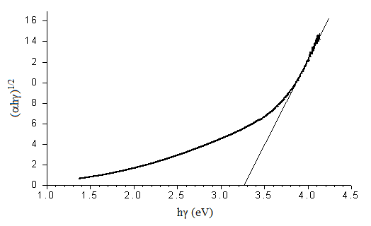
Figure 6: The absorption spectra of nco TiO2/SnO2 film prepared with SnCl4 rate of 35% in the initial solution mixture. Figure 7 shows the dependence of (hγ) 1/2 under hγ photon energy calculated from absorption coefficient in Figure 6. Linear extrapolation in the high photon energy absorption region to value of = 0 we obtain band gap width of Eg ~ 3.25 eV.
![Figure 7: Dependence (hγ)1/2 on hγ photon energies of the nco TiO2/SnO2 film prepared, which prepared with SnCl4 rate of 35% mol. Thus for nco TiO2/SnO2 film has the band gap reduced respectively compared with that prepared TiO2 film ~ 0.1 eV. This is caused by the presence of SnO2 phase during pyrolysis process to film formation, a number of Sn atoms was taken into TiO2 network kept role of impurities and / or generate oxygen vacancy in the network. Luminescence spectra of nco TiO2/SnO2 film prepared with 35% mol SnCl4 in the initial solution mixture is shown in Figure 8. The fluorescent spectrum of nano TiO2 films [13] had the same shape, but the maximum region of spectrum translated on visible light spectrum region and the peak had redshift 17 nm - 411.5 nm wavelength compared with 394.5 nm. Maximum spectrum also experienced in a broad region similar spectrum of luminescent nano TiO2 film is due to the superposition of different luminescence peaks. The entire maximum region of the spectrum shifted also demonstrates the spectrum peak shift. Thus, the shift of luminescent and absorption spectrum to the visible light region is related to the change of band gap width, the energy levels of impurities and the exciton binding energy levels in the forbidden band of nco TiO2/SnO2 films compared to TiO2 films.](/fulltextimages/384/fig_7.png)
Figure 7: Dependence (hγ)1/2 on hγ photon energies of the nco TiO2/SnO2 film prepared, which prepared with SnCl4 rate of 35% mol. Thus for nco TiO2/SnO2 film has the band gap reduced respectively compared with that prepared TiO2 film ~ 0.1 eV. This is caused by the presence of SnO2 phase during pyrolysis process to film formation, a number of Sn atoms was taken into TiO2 network kept role of impurities and / or generate oxygen vacancy in the network. Luminescence spectra of nco TiO2/SnO2 film prepared with 35% mol SnCl4 in the initial solution mixture is shown in Figure 8. The fluorescent spectrum of nano TiO2 films [13] had the same shape, but the maximum region of spectrum translated on visible light spectrum region and the peak had redshift 17 nm - 411.5 nm wavelength compared with 394.5 nm. Maximum spectrum also experienced in a broad region similar spectrum of luminescent nano TiO2 film is due to the superposition of different luminescence peaks. The entire maximum region of the spectrum shifted also demonstrates the spectrum peak shift. Thus, the shift of luminescent and absorption spectrum to the visible light region is related to the change of band gap width, the energy levels of impurities and the exciton binding energy levels in the forbidden band of nco TiO2/SnO2 films compared to TiO2 films.
![Figure 8: Luminescence spectra of nco TiO2/SnO2 film excited at 330 nm wavelength. The results of absorption and luminescent spectrum measurement on nco TiO2/SnO2 films showed a clear decline of the band gap compared with TiO2 film. This effect is not due to the contribution of SnO2, because this material has a larger band gap (3.8 eV). The decline of the TiO2 band gap caused by the presence of SnO2 phase is explained by the tendency to form rutile phase [18]. This phase band gap is of 3.0 eV. So nco TiO2/SnO2 films with high SnCl4 levels when prepared has a smaller band gap than TiO2 films. Determining a number of electrical parameters of nco TiO2/SnO2 film: Resistivity measurements of the film surface with measurements based on Hall effect gave results~ 725/, with a thickness of less than 0.5 μm film (carried out on Alpha step IQ KLA – CTENCOR meter), if infered conductivity, the value of this is greater than about 11-12 grades in comparison with the conductivity value of nano TiO2 film which was 10-10 (.cm)-1 by authors of the work [19] determined. The conductivity of the nco TiO2/SnO2 film as explained above, is caused by phase SnO2. The measurement results on carrier concentration of the nco TiO2/SnO2 film surface based on data from the measurements of resistivity and Hall effect for surface carrier concentration value were average ~ 1,4.1015/cm2. The average thickness of the film was prepared under 1m. Thus, the average carrier concentration of nco TiO2/SnO2 film was greater than value 1,4.1019/cm3. This value is smaller than 1-2 grates from films SnO2: F of the authors [11] prepared by spray pyrolysis method.](/fulltextimages/384/fig_8.png)
Figure 8: Luminescence spectra of nco TiO2/SnO2 film excited at 330 nm wavelength. The results of absorption and luminescent spectrum measurement on nco TiO2/SnO2 films showed a clear decline of the band gap compared with TiO2 film. This effect is not due to the contribution of SnO2, because this material has a larger band gap (3.8 eV). The decline of the TiO2 band gap caused by the presence of SnO2 phase is explained by the tendency to form rutile phase [18]. This phase band gap is of 3.0 eV. So nco TiO2/SnO2 films with high SnCl4 levels when prepared has a smaller band gap than TiO2 films. Determining a number of electrical parameters of nco TiO2/SnO2 film: Resistivity measurements of the film surface with measurements based on Hall effect gave results~ 725/, with a thickness of less than 0.5 μm film (carried out on Alpha step IQ KLA – CTENCOR meter), if infered conductivity, the value of this is greater than about 11-12 grades in comparison with the conductivity value of nano TiO2 film which was 10-10 (.cm)-1 by authors of the work [19] determined. The conductivity of the nco TiO2/SnO2 film as explained above, is caused by phase SnO2. The measurement results on carrier concentration of the nco TiO2/SnO2 film surface based on data from the measurements of resistivity and Hall effect for surface carrier concentration value were average ~ 1,4.1015/cm2. The average thickness of the film was prepared under 1m. Thus, the average carrier concentration of nco TiO2/SnO2 film was greater than value 1,4.1019/cm3. This value is smaller than 1-2 grates from films SnO2: F of the authors [11] prepared by spray pyrolysis method.
Hall Effect measurement of carrier mobility versus magnetic field intensity used into the pattern is shown in Figure 9. The results for electron mobility were μ ~ 7,5 cm2/V.s. This value is at the same grade but much greater than the value of the authors [19, 20, 21] and is located close to the range of values μ of the film SnO2: F prepared by spray pyrolysis method of the authors [11]. Electron mobility of nco TiO2/SnO2 film prepared in the range of intermediary between the mobility of the TiO2 anatase polycrystalline film was from 0.1-4 cm2/V.s [22] and the SnO2 film had average value of about 16 cm2/V.s [11]. TiO2/SnO2 system had composite form structure to the TiO2 and SnO2 phases alternating. Mobility in the system is effective mobility μe was calculated according to the expression [23]:
1/μe = 1/μTiO2 + 1/μSnO2
![Figure 9: The results for electron mobility were μ ~ 7,5 cm2/V.s. This value is at the same grade but much greater than the value of the authors [19-21] and is located close to the range of values μ of the film SnO2: F prepared by spray pyrolysis method of the authors [11]. Electron mobility of nco TiO2/SnO2 film prepared in the range of intermediary between the mobility of the TiO2 anatase polycrystalline film was from 0.1-4 cm2/V.s [22] and the SnO2 film had average value of about 16 cm2/V.s [11]. TiO2/SnO2 system had composite form structure to the TiO2 and SnO2 phases alternating. Mobility in the system is effective mobility μe was calculated according to the expression [23]:](/fulltextimages/384/fig_9.png)
Figure 9: The dependence of the carrier mobility of nco TiO2/SnO2 film versus the magnetic field. The mobility values of carriers obtained for nco TiO2/SnO2 film follow this rule. The value of the carrier concentration on the surface can also be explained by the same rules of the resistor in parallel. From these results it may be say that the system TiO2 and SnO2 material prepared by next pyrolysis method is composite system with two characteristics including - SnO2 phase and TiO2 particles are interspersed. - TiO2 is formed with a tendency of anatase phase transition into rutile in the presence of SnO2.
Ultraviolet light activated TiO2 causes the carrier appeared. Surrounded SnO2 phase also reduces the potential barriers between the TiO2 nanoparticles. The photoelectrons can thus move from one particle to another in creating a photocurrent generation in TiO2/SnO2 system.
Conclusion
By co-pyrolysis method from TiCl4 and SnCl4 salts, the nco TiO2/SnO2 film may be produced. Nco TiO2/SnO2 film can conduct electricity in normal lighting conditions, this opens a possibility of extending the applications of the film in the fields of photocatalysis and optoelectronics.
References
-
Guoguang L, Xuezhi Z, Yajie X, Xinshu N, Liqing Z, et al. (2005) The preparation of Zn2+-doped TiO2 nanoparticles by sol-gel and solid phase reaction methods respectively and their photocatalytic activities. Chemosphere 59(9): 1367-1371.
-
Shanmugasundaram Sakthivel, Marcin Janczarrek, Horst Kisch (2004) Visible light activity and photoelectrochemical properties of nitrogen-doped TiO2. J Phys Chem B 108(50): 19384-19387.
-
Yanqin Wang, Yanzhong Hao, Humin Cheng, Jiming Ma, Bin Xu, et al. (1999) The photoelectrochemistry of transition metal-ion-doped TiO2 nanocrystalline electrodes and higher solar cell conversion efficiency based on Zn2+-doped TiO2 electrode. J Mater Sci 34: 2773-2779.
-
Chang WY, Lin YC, Ke WW, Hsieh YS, Kuo NH (2005) Combined TiO2/SnO2 material with adding Pt by sol- gel technology for humidity sensor. Progress on Advanced Manufacture for Micro/Nano Technology 505-507(2): 397-402.
-
Jeremy Wade (2005) An Investigation of TiO2- ZnFe2O4 Nanocomposites for Visible Light Photocatalysis. Mas Thesis Electrical Engineering College of Engineering University, South Florida.
-
Jianxun Qiu, Mingyuan Gu (2005) Magnetic nanocomposite thin films of BaFe12O19 and TiO2 prepared by sol-gel method. Applied Surface Science 252(4): 888-892.
-
Ping Yang, Cheng Lu, Nanping Hua, Yukou Du (2002) Titanium dioxide nanoparticles co-doped with Fe3+ and Eu3+ ions for photocatalysis. Materials Letters 57(4): 794-801.
-
Yubai Bai, Liu Zhaoyue, Pan Kai, Zhang Qinglin, Liu Min, et al. (2004) The performances of the mercurochrome-sensitized composite semiconductor photoelectro-chemical cells based on TiO2/SnO2 and ZnO/SnO2 composites. Thin Solid Film 468(1-2): 291- 297.
-
Soliman Moataz, Hussein Mohamed M, El Atawy Samir, El Gamal Mohamed (2001) Effect of fluorine doping and spraying technique on the properties of tin oxide films. Renewable Energy 23(3-4): 463-470.
-
Te HF, Win JC (2003) Effect of freon flow rate on tin oxide thin films deposited by chemical vapor deposition. Applied Surface Science 220(1-4): 175- 180.
-
Thangaraju B (2002) Structural and electrical studies on highly conducting spray deposited fluorine and antimony doped SnO2 thin films from SnCl2 precursor. Thin Solid Films 402(1-2): 71-78.
-
Sathyamoorthy R, Sudhagar P, Chandramohan S, Vijayakumar KP (2007) Photoelectrical properties of crystalline titanium dioxide thin films after thermo- annealing. Crys Res Tech 42(5): 498-503.
-
Cuong Tran Kim (2015) Photoelectric Characteristics of Nano TiO2 Film Prepared By Spraying Pyrolysis Method. Int J Nano Stud Technol 4(1): 78-83.
-
Mogyorósi K, Dékány I, Fendler JH (2003) Preparation and Characterization of Clay Mineral Intercalated Titanium Dioxide Nanoparticles. Langmuir 19(7): 2938-2946.
-
Barakat MA, Schaeffer H, Hayes G, Ismat Shah S (2005) Photocatalytic degradation of 2-chlorophenol by Co-doped TiO2 nanoparticles. Applied Catalysis B Environmental 57(1): 23-30.
-
Guha S, Ghosh K, Keeth JG, Ogale SB, Shinde SR, et al. (2003) Temperature-dependent optical studies of Ti1- xCoxO2. Appl Phys Lett 83(16): 3296-3298.
-
Linsebigler AL, Lu G, Yates JT (1995) Photocatalysis on TiO2 surfaces: Principles, mechanism, and selected results. Chem Rev 95(3): 735-758.
-
Mahanty S, Roy S, Suchitra Sen (2004) Effect of Sn doping on the structural and optical properties of sol- gel TiO2 thin films. Journal of crytal growth 261(1): 77-81.
-
Nickolay Golego, Studenikin SA, Michael Cocivera (1998) Bandgap DOS Distribution From Transient Photoconductivity in Thin-Film Polycrystalline TiO2 Containing Nb, The 53rd Congress of Canadian Association of Physicists, University of Waterloo, Canada.
-
Boston Electronics Corporation (2002) TiO2 UV photodiodes.
-
Simon Springer (2004) Free carriers in nanocrystalline titanium dioxide thin films. Sci Doc Thesis of Physisc, École polytechnique Fédérale de Lausanne, France.
-
Shang Di Mo, Ching WY (1995) Electronic and optical properties of three phases of titanium dioxide: rutile, anatase, and brookite. Phys Rev B Condens Matter 51(19): 13023-13032.
-
Kuchik EV (1974) Investigation Methods of Hall Effect. SoViet Radio Publis.
- Solution-Processed Chiral Perovskites for Biomedical Applications
- Nanotechnology in Health Chemistry and Medicine: Current Challenges and Future Directions
- Human Exposure to Micro- and Nanoplastics: Pathways, Toxicity, and Intervention Strategies
- Exosome Nanomedicine for Cancer Therapy
- Micro and Nanoplastics–Plastisphere, Biotoxicity, Impact on Human Health, and Mitigation Strategies
- Process Validation of Cefixime Powder for Suspension Dosage Form, 50 mL