Thin Film Chromium Coating on Glass Substrate Optimized By Taguchi Method
The sputtering technique used for deposition of thin film metallized product onto base substrate material. The experiment was conducted to deposit thin film Cr-coating on glass substrate with varying process parameters. The design of experiment (DOE) was conducted to optimize the process parameters to achieve defect-free coating on glass substrate. Taguchi fractional factorial orthogonal array was used to perform DOE & ANOVA analysis. The deposition of chromium metal on glass substrate was used during the experiments conducted. The results of the experiments were evaluated against quality of the coating and the thickness. Detailed ANOVA analysis has been performed to standardize the variables.
Introduction
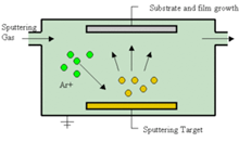
Sputtering is a physical vapor deposition process in vacuum in which one material is coated on another. The material which is deposited or coated is called the target and the material on which it is coated is called the substrate. The target is bombarded with ions, which transfer momentum and kinetic energy to the target particles, and the target particles move and get deposited on the substrate [1].
The target is kept on the cathode and the substrate is kept on the anode. The chamber is first made to vacuum, after which argon gas is pumped in. When a negative voltage is applied to the target, plasma is formed, and argon gas is ionized. The positive argon ions hit the target and pass on momentum and kinetic energy to the target atoms. The target atoms gets ejected and deposited on the substrate. Thus, the target atoms are coated on the substrate [1] (Figure1).
Sputtering is an extremely useful technique for thin film coating. It is used in the deposition of various thin films in integrated circuit processing, magnetic hard drives etc. It is also used for making antireflective (AR) coatings and low emissivity coatings on glass. Sputtering is used for coating of contact metals for thin film transistors. It is used for the fabrication of CDs and DVDs and in the manufacture of optical waveguides. Sputtering is also used for making efficient photovoltaic solar cells.
There are several types of sputtering such as RF- sputtering, and DC magnetron sputtering. DC magnetron sputtering has been used in this paper. Magnetron sputtering uses magnets behind the cathode to trap electrons, so that they don’t bombard the substrate and deposition takes place faster and more efficiently. The magnets can be of rectangular or circular and can be arranged in different ways. Circular magnets in confocal arrangement were used in the experimentation [1].
Based on the type of source (power supply), sputtering can be of different types like DC and RF sputtering. In DC sputtering, the supply is DC while in RF sputtering the supply is AC with radio frequency. DC sputtering can be used for coating metals, but cannot be used for coating insulators, non-metallic, dielectrics as charge build up over time in these materials are not possible. Therefore, RF sputtering is used in such cases, which alternates the electric charge at radio frequency to prevent charge build up. The DC sputtering methodology has been used within the scope of this study [1, 2, 3].
There are many parameters which affect sputtering. The following is a list of the same.
- Power
- Process Pressure
- Distance between target and substrate
- Rotation (RPM) of substrate holder
- Time
- Substrate Temperature
- Argon Gas Flow Rate
- Argon gas pressure
- Argon Gas Grade
- Target Composition
- Target Angle
- Target thickness
- Substrate
- Magnet configuration
- Ion cleaning
- Vacuum System
- Atmosphere.
The following defects are normally evident in coating and seen in literature [4, 5].
- Nodules and Bumps
- Plateau or Occluded particles
- Voids or Pinholes
- Depressions or Pits
- Scratches
- Stains, spots and contaminations
- Blisters
- Edge Rolling Based on the literature survey, the following parameters can be measured as per the methodology explained herewith and to identify the certain usage of thin-film metallized devices.
Thickness
Thickness of the film is a very important parameter in metallized devices. One way to measure the thickness of the film is to use Profilometer. It is used to measure the surface’s profile. AFM (Atomic Force Microscope) can also be used to measure the thickness. AFM is a very high-resolution type of scanning probe microscope. It can be used for imaging and get a 3d model of the surface, which gives the surface topography and hence the thickness. Another tool to measure the thickness is Scanning near-field optical microscopy (SNOM). By masking tape on one part of the substrate and preventing it from getting coated, we can find the step in the surface profile between the coated and the uncoated part and hence to measure the thickness of the coated material [6, 7].
Thickness Uniformity
Thickness uniformity can also be measured using a Profilometer, AFM or SNOM. Even XRF and SEM (Scanning Electron Microscope) can be used. By characterizing the surface topography, we can find how uniform the coating is [6, 7].
Sheet Resistance
Sheet resistance (also known as surface resistance or surface resistivity) is a common electrical property used to characterize thin films of conducting and semiconducting materials. It is a measure of the lateral resistance through a thin square of material, i.e. the resistance between opposite sides of a square. This is measured for electrical circuits, to find the uniformity of the conductive layer. The primary technique for measuring sheet resistance is the four-probe method (also known as the Kelvin technique), which is performed using a four-point probe. It operates by applying a current (I) on the outer two probes and measuring the resultant voltage drop between the inner two probes which then gives the sheet resistance using an equation. Sheet resistance measurements are also commonly done with an eddy-current gauge. An inductive circuit generates a high frequency magnetic field, which causes circulating eddy- currents in the wafer. These currents cause a power loss, which is detected by the gauge and is used to calculate sheet resistivity which can then give the sheet resistance [8-
11].
Defects
The defects listed above can be visually inspected by using a zoom microscope or SEM or AFM. These high- resolution microscopes can be used to identify the defects. We can get an image of the surface and measure the diameter and size of the various defects [1].
Adhesion
Adhesion is a measure of how well the coating has been applied. One test is to attach some pulling device to the back of the film and then pull the film using a tensile tester method. The above method is called direct pull-off method. Another way it can be measured is by pressing a pressure sensitive tape on the coated material and then rapidly stripping it off to see how much has been detached. The above test is called the scotch-tape method. There are other methods to measure the force to remove the coated part. The more the force, the more is the adhesion. Another test is the Peel test, in which the coated film is peeled off, and the work done, or energy is measured. Another test is the scratch or scribe test, where a diamond tip is drawn across the film surface and a load is applied to the point. The value of the load at which the film breaks is a measure of the adhesion.
Optical Measurements
The reflectance, transmittance and absorbance are measured for use in various optical devices. The reflectance of the thin film can be measured using a reflectance spectrometer. This will measure how uniformly the film is coated. The main method used for measuring optical properties is spectrometry. To optimize the sputtering process for thin film metallization coating, the Taguchi fractional factorial method is used for Design of Experiment (DOE). This method is useful as one need to perform fewer experiment. This method uses a set of arrays called the orthogonal arrays. The important part of the orthogonal array method is to pick the level combinations of the input variables for each experiment. This is done based on the number of factors and the number of levels of each factor. For example, for 4 factors with 3 levels each, the L9 orthogonal array can be used in which only 9 experiments are to be done instead of 81. Hence the major advantage of this method is that this method cuts down the time and cost for the analysis. The interactions between two factors can also be taken as a factor [12, 13].
All the level settings appear in equal number of times. For example, in the L9 array for variable 4, level 1, level 2 and level 3 appears thrice. This is known as the balancing property of orthogonal arrays. All the level values of the independent variables are used for conducting the experiments.
The sequence of level values for conducting the experiments should not be changed. That means one cannot conduct experiment 1 with variable 1, level 2 setup and experiment 4 with variable 1, level 1 setup. The reason for this is that the array of each factor columns is mutually orthogonal to any other column of values.
The degree of freedom for each factor is one less than the number of levels of that factor. The minimum number of experiments required in this method is 1 more than the sum of degree of freedoms of each factor. After the experiments are conducted and the data is collected, analysis is done to find out how each factor contributes to the result. Noise analysis can be conducted for other fluctuating parameters.
The main advantages of this method are that lesser number of runs are needed and also gives a mean value for the required result. The major disadvantage is that the results obtained are relative and the parameter with highest importance is not indicated. Also the interactions between the parameters are not well accounted.
Materials and Methods
The glass substrate and chromium target were selected. The coating was done under various conditions and the quality characteristics and thickness were measured.
The factors (parameters) which were selected for the DOE were Power, Distance between target and substrate, Time and the Gas flow rate. For each factor 3 levels were selected. The following table shows the factors and the levels selected (Table 1).
| Factor | Level -1 | Level - 2 | Level - 3 | DOF |
|---|---|---|---|---|
| Power (Watts) – [A] | 100 | 125 | 150 | 2 |
| Distance(mm) – [B] | 90 | 120 | 150 | 2 |
| Time(min) – [C] | 15 | 30 | 45 | 2 |
| Gas flow(sccm) – [D] | 25 | 30 | 35 | 2 |
Table 1: Factors and Levels in DOE.
Each experiment was conducted in the following way. The substrate was appropriately cleaned by using DI water, acids, alkalis and organic solvents and vapor degreasing was finally performed in organic solvent medium. The distance between the substrate and target was set and the substrate was then loaded into the vacuum chamber and the chamber is brought to vacuum using 2 pumps – the mechanical pump and the turbomolecular pump. The mechanical scrolled pump brought down the pressure at 10-3 torr, and the turbomolecular pump brought down the pressure from 10-3 torr to 10-7 torr. The parameters – power, gas flow rate and the speed of rotation (20 rpm) of the substrate were set and then the sputtering process was performed. After the requisite time, the sputtering process was stopped, and the chamber was vented to take out the coated substrates.
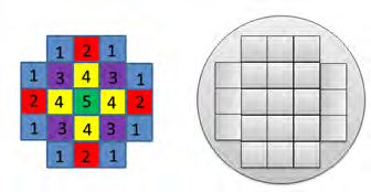
21 substrates (1” x 1”) are used in the sample holder as shown in the fig. 2 below. While the substrate holder is under rotation, few positions are equivalent towards sputtering. The equivalent substrates are depicted with the same color and numbers as shown in Figure 2.
Thus substrates were selected from different location and the thickness and quality characteristics (number of voids) were measured.
The Taguchi method was used to analyze the effect of the different factors at different level. Since there are 4 factors with 3 levels each, 9 experiments were conducted. The following was the orthogonal array used (Table 2).
The defects observed were edge rolling, scratches, stains and voids. The number of voids was quantified. For each batch (experiment), 5 samples from different locations were analyzed under a stereo zoom microscope (optical microscope), and the number of voids were visually calculated. Each batch was given a ranking from 0 using its average, with 0 being the most defective, by normalizing it with the most defective sample and setting that to 0. DOE with Taguchi method was performed on this ranking.
| A | B | C | D | |
|---|---|---|---|---|
| 1 | 1 | 1 | 1 | 1 |
| 2 | 1 | 2 | 2 | 2 |
| 3 | 1 | 3 | 3 | 3 |
| 4 | 2 | 1 | 2 | 3 |
| 5 | 2 | 2 | 3 | 1 |
| 6 | 2 | 3 | 1 | 2 |
| 7 | 3 | 1 | 3 | 2 |
| 8 | 3 | 2 | 1 | 3 |
| 9 | 3 | 3 | 2 | 1 |
Table 2: Orthogonal Array for the DOE experimentation.
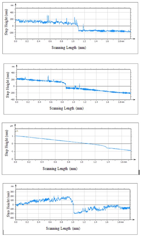
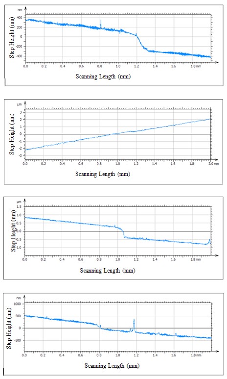
One sample was taken from each batch and the average coating thickness was measured using a Profilometer Alpha Step D600 of KLA Tencor, USA.
Results and Discussion
Calculations for Doe
• For factors, DOF = number of levels – 1
• For total, DOF = number of readings – 1
- For error, DOF = DOF of total – sum of DOF for each factor
- CF = (Sum of all observations)2/(number of observations)
- SS for each factor = (sum of all observations when factor at level 1)2/(number of observations when factor at level 1) + (sum of all observations when factor at level 2)2/ (number of observations when factor at level 2) + (sum of all observations when factor at level 3)2/(number of observations when factor at level 3) – CF
- SS for total = Sum of square of each observation – CF
- SS for error = SS for total – sum of SS for each factor
- MS = SS/DOF for factors and error
- F-Cal for each factor = MS of the factor/MS of error
- F-tab for each factor is got from table using the DOF of factor and DOF of error
- If the F-cal > F-tab, the factor contributes to the DOE
- % contribution of each factor = (SS of each factor – DOF of factor *MS of error)*100/(SS of total). The average value of each factor at each level is used to make conclusions.
Quality Ranking Qualification for Each Experimentation
| Exp No \ Factor | A | B | C | D | Position | Position | Position | Position | Position | Average | Ranking |
|---|---|---|---|---|---|---|---|---|---|---|---|
| No. 1 | No.2 | No. 3 | No. 4 | No. 5 | |||||||
| 1 | 1 | 1 | 1 | 1 | 3 | 6 | 5 | 4 | 4 | 4.4 | 5.0 |
| 2 | 1 | 2 | 2 | 2 | 6 | 10 | 5 | 6 | 6 | 6.6 | 2.5 |
| 3 | 1 | 3 | 3 | 3 | 3 | 1 | 2 | 1 | 2 | 1.8 | 7.9 |
| 4 | 2 | 1 | 2 | 3 | 1 | 2 | 3 | 5 | 4 | 3 | 6.6 |
| 5 | 2 | 2 | 3 | 1 | 1 | 3 | 2 | 2 | 4 | 2.4 | 7.3 |
| 6 | 2 | 3 | 1 | 2 | 2 | 5 | 7 | 4 | 8 | 5.2 | 4.1 |
| 7 | 3 | 1 | 3 | 2 | 6 | 8 | 10 | 6 | 14 | 8.8 | 0 |
| 8 | 3 | 2 | 1 | 3 | 6 | 8 | 5 | 2 | 6 | 5.4 | 3.9 |
| 9 | 3 | 3 | 2 | 1 | 1 | 7 | 3 | 12 | 2 | 5 | 4.3 |
Table 3: Results of the quality ranking in each experimentation.
| Source ff Variation | DOF | SS | MS | FCAL | FTAB | Contributes | %Contribution |
|---|---|---|---|---|---|---|---|
| Factor A | 2 | 85.92 | 42.95 | 6.8 E+15 | 3.26 | Yes | 35 |
| Factor B | 2 | 19.11 | 9.55 | 1.5E+14 | 3.26 | Yes | 8 |
| Factor C | 2 | 4.820 | 2.41 | 3.8 E+14 | 3.26 | Yes | 2 |
| Factor D | 2 | 134.98 | 67.49 | 1.1E+16 | 3.26 | Yes | 55 |
| Error | 36 | 0.00 | 0.00 | ||||
| Total | 44 | 244.83 | 100 |
Table 4: ANOVA table for the quality ranking in each experimentation.
Since for all the factors, the calculated f value was greater than the f with the tabulated one, all the factors contribute, but the major contributor was found to be the gas flow which was followed by the power.
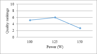
| Power | Average ranking |
|---|---|
| 100 W | 5.151515 |
| 125 W | 5.984848 |
| 150 W | 2.727273 |
Table 6: Effect of the Factor – Power on ranking.
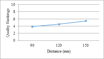
| Distance | Average ranking |
|---|---|
| 90mm | 3.863636 |
| 120mm | 4.545455 |
| 150mm | 5.454545 |
Table 5: Effect of the Factor – Time on ranking.
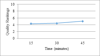
| Time | Average ranking |
|---|---|
| 15 min | 4.318182 |
| 30 min | 4.469697 |
| 45 min | 5.075758 |
| Gas flow | Average ranking |
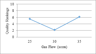
| 25 sccm | 5.530303 |
| 30 sccm | 2.19697 |
| 35 sccm | 6.136364 |
Table 7: Effect of the Factor – Time on ranking.
The average value of the ranking was plotted against the respective factors at each level and the following plots were obtained (Figure 3).
- For the given factors and levels, the ranking first increases for power from 100W to 125W and then decreases from 125W to 150W.
- For the given factors and levels, the maximum ranking occurs at 125W (Figure 4).
- For the given factors and levels, the ranking increases for distance from 90mm to 150mm
- For the given factors and levels, the maximum ranking occurs at 150mm (Figure 5).
- For the given factors and levels, the ranking increases for time from 15min to 45min
- For the given factors and levels, the maximum ranking occurs at 45 min (Figure 6).
- For the given factors and levels, the ranking first decreases for gas flow from 25sccm to 30sccm and then increases from 30sccm to 35sccm.
- For the given factors and levels, the maximum ranking occurs at 35sccm.
From the above we can see that the optimum combination to reduce the number of voids and have quality coatings is Power -125 W, Distance between target and substrate – 150mm, Time - 45min and gas flow – 35sccm.
The results of the confirmatory experiment conducted is as follows.
Results of the confirmatory experiment
| Sample ID | Position No. 1 | Position No. 2 | Position No. 3 | Position No. 4 | Position No. 5 | Quality Ranking |
|---|---|---|---|---|---|---|
| No of Voids | 2 | 2 | 2 | 1 | 2 | 7.95 |
Table 8: Effect of the Factor-Gas Flow on ranking the thickness data as measured for this confirmatory trial is 3589.04 Angstrom
| Experiment - 1 | Experiment - 2 |
| Experiment – 3 | Experiment - 4 |
| Experiment - 5 | Experiment - 6 |
| Experiment - 7 | Experiment - 8 |
| Experiment - 9 | Confirmatory Experiment |
Table 9: Optical Microstructure Images for the DOE experimentation.
Thickness Quantification for Each Experimentation
| Factor | A | B | C | D | Thickness (in mm) |
|---|---|---|---|---|---|
| 1 | 1 | 1 | 1 | 1 | 0.0001246 |
| 2 | 1 | 2 | 2 | 2 | 0.0001831 |
| 3 | 1 | 3 | 3 | 3 | 0.0002693 |
| 4 | 2 | 1 | 2 | 3 | 0.0003704 |
| 5 | 2 | 2 | 3 | 1 | 0.0003806 |
| 6 | 2 | 3 | 1 | 2 | 0.0001166 |
| 7 | 3 | 1 | 3 | 2 | 0.0005666 |
| 8 | 3 | 2 | 1 | 3 | 0.0001706 |
| 9 | 3 | 3 | 2 | 1 | 0.0002840 |
| Source of Variation | Df | Ss | Ms | %Contribution | |
| Factor A | 2 | 10.18E-8 | 5.09E-8 | 20 | |
| Factor B | 2 | 8.82E-8 | 4.41E-8 | 17 | |
| Factor C | 2 | 32.41E-8 | 16.21E-8 | 63 | |
| Factor D | 2 | 0.32E-8 | 0.16E-8 | 1 | |
| Error | 36 | 0.0E-8 | 0E-8 | ||
| Total | 44 | 51.73E-8 | 100 |
Table 10: Thickness results for the DOE experimentation. (Thickness as measured by surface profilometer – Alpha Step D600 model of
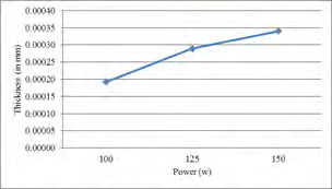
| Power | Average thickness |
|---|---|
| 100 W | 0.00019 |
| 125 W | 0.00029 |
| 150 W | 0.00034 |
Table 11: Effect of the Factor – Power on thickness (mm).
| Distance | Average thickness |
|---|---|
| 90mm | 0.00035 |
| 120mm | 0.00024 |
| 150mm | 0.00022 |
Table 14: Effect of the Factor – Distance on thickness (mm).
| Time | Average thickness |
|---|---|
| 15 min | 0.00014 |
| 30 min | 0.00028 |
| 45 min | 0.00041 |
Table 12: Effect of the Factor – Time on thickness (mm).
| Gas flow | Average thickness |
|---|---|
| 25 sccm | 0.00026 |
| 30 sccm | 0.00029 |
| 35 sccm | 0.00027 |
Table 13: Effect of the Factor – Gas flow on thickness (mm).
The average value of the thickness was plotted against the respective factors at each level and the following plots were obtained (Figure 7).
- For the given factors and levels, the thickness first increases for power from 100W to 150W
- For the given factors and levels, the maximum thickness occurs at 150W (Figure 8).
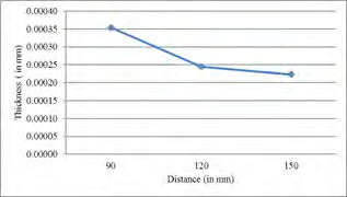
- For the given factors and levels, the thickness first decreases for distance from 90mm to 150mm.
- For the given factors and levels, the maximum thickness occurs at 90mm (Figure 9).
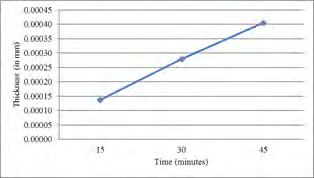
- For the given factors and levels, the thickness increases with time from 15 minutes to 45 minutes.
- For the given factors and levels, the maximum thickness occurs at 45minutes (Figure 10).
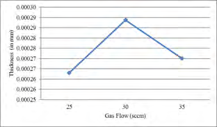
• For the given factors and levels, the thickness first increases for gas flow from 25 sccm to 30sccm and then decreases from 30 sccm to 35 sccm.
• For the given factors and levels, the maximum thickness occurs at 30 sccm (Figure 11).
Experiment – 1
Experiment – 2
Experiment – 3
Experiment – 4
Experiment – 5
Experiment – 6
Experiment – 7
Experiment – 8
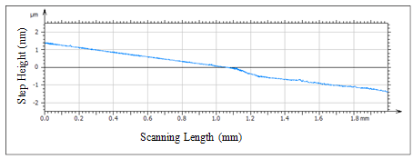
Experiment - 9 Figure 11: Surface profilometer scan report for the thickness measurement (Experiment-1 to Experiment -9) The above results are valid only for the levels and factors taken. Both the DOEs were done to 95% accuracy.
Conclusion
The quality of coating was visually studied under zoom microscope and has been optimized for getting the least number of defects (voids) in the present combination of factors and levels. The optimum combination of power applied is 125 W, while distance between the target and substrate holder is 150 mm and the optimum time is 45 min for the given coating with the gas flow of 35 sccm.
The coating thickness average was measured from each batch and the relationship graph is arrived and plotted.
In future, we can improve upon the relationship and its related trend, by taking into consideration of thickness uniformity within a sample and also considering the measurement of thickness from different samples across the substrate holder. The future scope is to vary the factors and to carry out DOE with newer levels.
References
-
Tan XQ, Liu JY, Niu JR, Liu JY, Tian JY (2018) Recent Progress in Magnetron Sputtering Technology used on Fabrics. MDPI 11(10): 1953.
-
Hones P, Diserens M, Levy F (1999) Characterization of sputter-deposited chromium oxide thin films. Surface and Coatings Technology 120: 277-283.
-
Jung YS, Lee DW, Jeon DY (2004) Influence of dc magnetron sputtering parameters on surface morphology of indium tin oxide thin films. Applied surface science 221(1- 4): 136-142.
-
Čekada M, Radić N, Jerčinović M, Panjan M, Panjan P (2017) Growth defects in magnetron sputtered PVD films deposited in UHV environment. Vacuum 138: 213- 217.
-
Kaushik P (2018) Sputtering Techniques. Indian Institute of Technology. Surface Engineering of Nanomaterials, Roorkee.
- Solution-Processed Chiral Perovskites for Biomedical Applications
- Nanotechnology in Health Chemistry and Medicine: Current Challenges and Future Directions
- Human Exposure to Micro- and Nanoplastics: Pathways, Toxicity, and Intervention Strategies
- Exosome Nanomedicine for Cancer Therapy
- Micro and Nanoplastics–Plastisphere, Biotoxicity, Impact on Human Health, and Mitigation Strategies
- Process Validation of Cefixime Powder for Suspension Dosage Form, 50 mL