Effect of Substrate Temperature on Structure, Morphology and Optical Properties of β-Ga2O3 Thin Film Grown on GaN by MBE
The structure, morphology and optical properties of β-Ga2O3 thin films grown on GaN at various substrate temperature by ozone molecular beam epitaxy (MBE) are investigated in this work. (-201)-oriented β-Ga2O3 thin films are formed on c-plane GaN template substrate. When the substrate temperature increases, the crystal quality of β-Ga2O3 thin film improves, and a high-crystalline-quality β-Ga2O3 thin film is obtained at the substrate temperature of 700 °C. The Φ scans of X-ray diffraction is utilized to characterize the β-Ga2O3 thin film, from the result we find that the β-Ga2O3 thin film has a six-fold domain structure, attributed to the epitaxial relationships (β-Ga2O3 [010] // GaN [11-20] and β-Ga2O3 [102] // GaN [1-100]). Base on the morphology, it can be seen that the β-Ga2O3 thin film follows the island-growth model, and the size of the island increases as the substrate temperature increases. Furthermore, it is found that the defect related luminescence decreases with the increase of substrate temperature by analyzing the CL spectra, implying the improvement of crystal quality. The presented optimized β-Ga2O3 thin film grown on GaN template substrate should effectively promote the development of high reliable performance self-powered ultraviolet (UV) photodetector based on the Ga2O3/GaN heterojunction.
Boyuan Feng1,3, Gaohang He1*, Zhengcheng Li1,3, Ying Wu1, Zhongming Zeng2 and Sunan Ding1,3
RMS: Root-Mean-Square; SEM: Scanning Electron Microscope; GL: Green Luminescence; BL: Blue Luminescence; DAP: Donor-Acceptor Pair.
Introduction
Driven by its potential application on high power electronics and solar-blind ultraviolet (UV) photodetectors (PDs), gallium oxide in its most thermodynamically stable monoclinic structure, β-Ga2O3, gradually enters people’s field of vision. Compared to GaN and SiC, β-Ga2O3 has a wide band gap (4.3-4.9 eV), high breakdown electric field (8 MV/ cm) and excellent Baliga’s figure (3214) [1, 2, 3, 4, 5]. Therefore, β-Ga2O3 is attracting interest for solar-blind self-powered UV PDs [6, 7, 8, 9, 10, 11], Schottky barrier diodes (SBDs) [12], metal- semiconductor field-effect-transistors (MESFETs) [2] and metal-oxide-semiconductor field-effect-transistors (MOSFETs) [13, 14, 15].
The possibility of depositing β-Ga2O3 films on native substrates grown from the melt can allow synthesis of high-quality films and large-scale production, nonetheless, the high price hinders its possible application. Hence, heteroepitaxial β-Ga2O3 films have been obtained on several substrates, such as α-Al2O3 (0001) [16, 17], MgO (100) [18], GaN (0001) [19, 20], STO (100) [21] and KTaO3 (100) [22]. At the same time, the corresponding photodetectors have been prepared and achieved excellent performance [23]. Among them, Guo, et al. [9, 10] prepared a heterojunction by depositing n-type β-Ga2O3 thin film on p-type GaN by pulse laser deposition (PLD) to realize a super-high-performance self-powered UV photodetector, which helped solve the energy issues. However, the β-Ga2O3 thin film grown on GaN by molecular beam epitaxy (MBE) have been investigated to date seldom.
Recently, Nakagomi, et al. [20] reported that the orientation of β-Ga2O3 thin film formed on GaN template substrate was found to be (-201) β-Ga2O3 || (0001) GaN || (0001) sapphire and (010) β-Ga2O3 || {11-20} GaN, resulting in six-fold domain structure of the β-Ga2O3 layer. The β-Ga2O3 film grown on GaN substrate by metal organic chemical vapor deposition (MOCVD) is amorphous and transformed into (100) crystalline phase by annealing in oxygen atmosphere [24]. Li, et al. [19] reported the growth of vertical β-Ga2O3 nanowire arrays on GaN layers by MOCVD. The effect of the growth temperatures on the β-Ga2O3 thin film formed on GaN substrate remained unexplored, which is one of the crucial parameters for achieving high crystalline quality. In this work, the influence of substrate temperatures on the film quality is studied by using the ozone MBE. In addition, the epitaxial relationships, morphology and the optical properties are analyzed.
Experiments
The β-Ga2O3 thin films on (0001) Ga-plane GaN template (4 μm on (0001) sapphire substrate) were deposited by a commercial MBE (Octoplus-O 400, Komponenten) with liquid Ga (99.9999%) and ozone as the Ga source and O source. The GaN template substrate was cleaned by ultrasonic agitation in acetone, isopropyl alcohol and deionized water for 15min each, followed by drying with nitrogen gas blowing. During the growth, the ozone pressure of growth chamber was maintained at 5×10⁻⁶mbar, and the Ga flux was 0.14Å/s which was detected by a quartz monitor crystal. The substrates were heated to growth temperature (500℃ ~ 700℃), and then growth for 3h.
X-ray diffraction (XRD; D8 Advanced, Bruker) was carried out to check out the crystalline orientations and crystal quality. The film thickness was determined by cross- section observation with a focused ion beam (FIB; Scios, FEI), meanwhile, the surface morphology of the film was obtained from the plane view. The surface roughness of the film was analyzed by atomic force microscopy (AFM; Asylum Research MFP-3D, Oxford). The optical properties of β-Ga2O3 films was characterized by scanning cathodoluminescence (CL; Delmic Sparc, FEI).
Results and Discussion
The XRD θ-2θ scans of β-Ga2O3 thin films prepared with different substrate temperatures are shown in Figure 1(a). After the deposition of β-Ga2O3 thin films with the temperature changed from 500 to 700 °C, three diffraction peaks appear and locate at 18.96°, 38.36° and 58.09°, respectively, which correspond to the (-201), (-402) and (-603) lattice planes of monoclinic β-Ga2O3 (PDF# 43-1012). This indicates that the (-201) planes in the β-Ga2O3 thin film are parallel to the (0001) GaN surface. In addition, when the substrate temperature is 500 °C, the unwanted plane of (-801) is shown in the XRD θ-2θ scan, demonstrating the polycrystalline nature of this film. As the increase of substrate temperature, the (-801) plane disappears, indicating that when the substrate temperature above 550 °C, the β-Ga2O3 thin film is grown with the single orientation along (-201) lattice plane on the GaN template substrate. Figure 1(b) shows the XRD rocking curves of the (-201) plane of the β-Ga2O3 thin films prepared at different growth temperatures. And the full width at half-maximum (FWHM) values of rocking curves are plotted as a function of the substrate temperature in Figure 1(c). Apparently, the FWHM value monotonically decreases with increasing growth temperature and down to 1.67° at 700 °C, implying excellent crystal quality and unique (-201) out-plane orientation of the thin film.
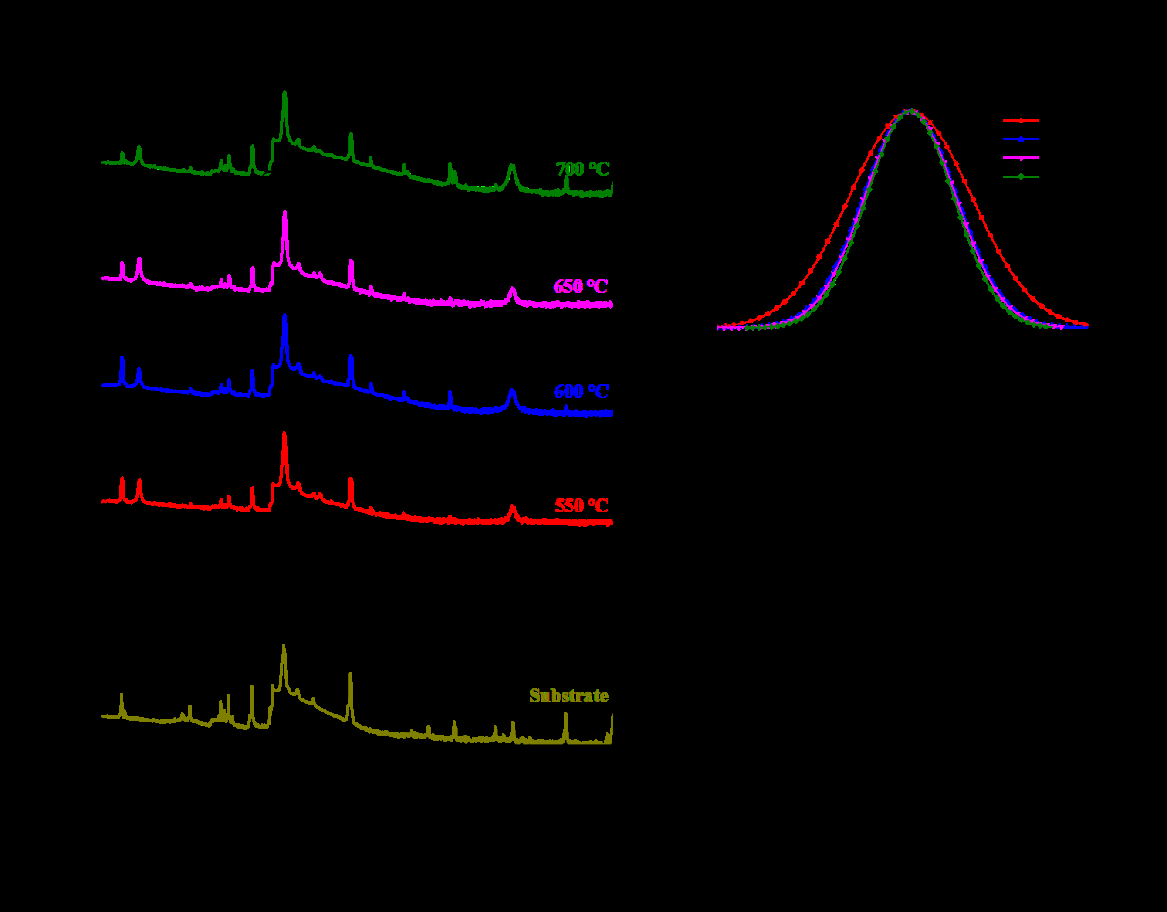
Figure 2(a) shows the XRD Φ-scan results for the β-Ga2O3 {-401} diffraction of the film grown at 700 ℃. It can be seen that there are 6 diffraction peaks, derived from the β-Ga2O3 {-401} diffraction with the rotation angle offset 30°. Furthermore the 6 peaks appear every 60° are observed from the six peaks which associated with the {11-22} diffractions of GaN. This result indicates that the β-Ga2O3 thin film has a six-fold domain structure and an epitaxial relationship with the GaN. The schematic diagram of epitaxial relationship is presented in Figure 2(b). Base on it one can get that epitaxial relationships between (-201) plane of β-Ga2O3 (orange) and (0001) plane of GaN (blue) are β-Ga2O3 [10] // GaN [11, 12, 13, 14, 15, 16, 17, 18, 19, 20] and β-Ga2O3 [102] // GaN [1, 2, 3, 4, 5, 6, 7, 8, 9, 10, 11, 12, 13, 14, 15, 16, 17, 18, 19, 20, 21, 22, 23, 24, 25, 26, 27, 28, 29, 30, 31, 32, 33, 34, 35, 36, 37, 38, 39, 40, 41, 42, 43, 44, 45, 46, 47, 48, 49, 50, 51, 52, 53, 54, 55, 56, 57, 58, 59, 60, 61, 62, 63, 64, 65, 66, 67, 68, 69, 70, 71, 72, 73, 74, 75, 76, 77, 78, 79, 80, 81, 82, 83, 84, 85, 86, 87, 88, 89, 90, 91, 92, 93, 94, 95, 96, 97, 98, 99, 100]. The appearance of six-fold domain structure is due to the three-fold rotation symmetry corresponds to the epitaxial relationship and the originally two-fold β-Ga2O3 epitaxial growth in the three different directions at same rates [20].
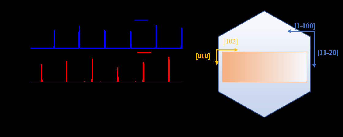
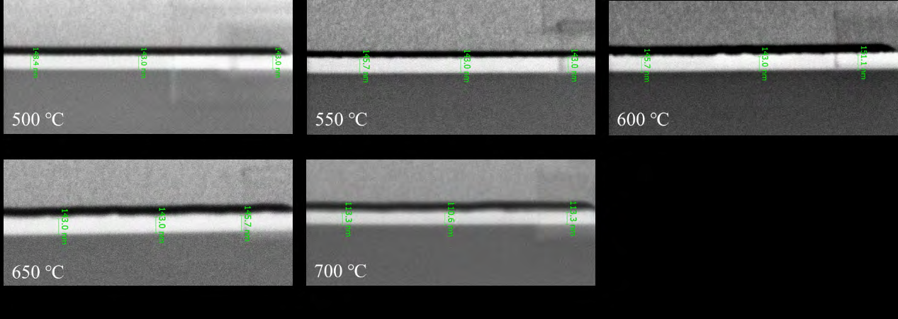
Figure 3 shows the cross-sectional scanning electron microscope (SEM) images of the β-Ga2O3 films prepared with different substrate temperatures and fabricated by FIB. The carbon layer and platinum layer are covered on the surface to are used to protect the surface before FIB. It can be seen that the thickness of film is stable around 144 nm. However, the film thickness decreases to 112 nm with the substrate temperature set at 700 ℃. This may be due to the enhanced of the desorption or evaporation rate of volatile Ga2O suboxide from the substrate when the temperature exceeds 700 ℃ [16, 25].
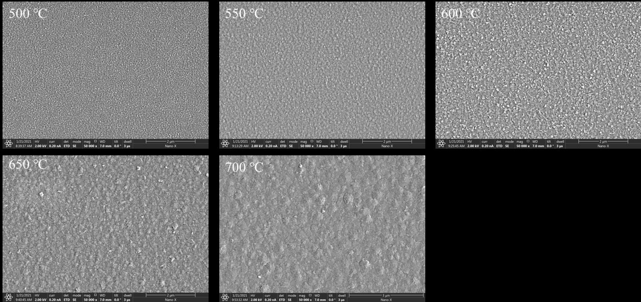
The SEM plane-view images of β-Ga2O3 thin films grown at various temperatures are shown in Figure 4. It can be clearly observed that the β-Ga2O3 thin film grown on GaN template substrate follows the island-growth model, and the island size of β-Ga2O3 thin film increases as the substrate temperature increases. We believe that the island size difference is ascribed to the growth mechanism with different substrate temperature. When the substrate temperature is fixed at 500 ℃, the adatoms do not have enough mobility, which limits the atomic migration distance and determine the size of the island. Thus, the polycrystalline thin film forms, which is consisted with the XRD results as shown in Figure 1(a). It is notable that the surface prefers a low free energy, the appeared morphology should be spherical shaped island, if the substrate structure is not similar to that of the epitaxial film. Hence, considering the influence of the substrate lattice structure, island structure appears as has been observed in the SEM images. Upon increasing the substrate temperature, the increased atomic mobility causes the radius of island to become larger, and nearby island begins to join together as shown in the SEM images.
Figure 5 displays the AFM morphologies and roughness of β-Ga2O3 thin films. The change of morphology is consistent with the SEM images with the substrate temperature increase. Corresponding to the changes of the surface morphology, the root-mean-square (RMS) roughness of the films increases when the substrate temperature does not exceed 650 ℃. The maximum roughness of the films is 6.15 nm, indicating smooth surface.
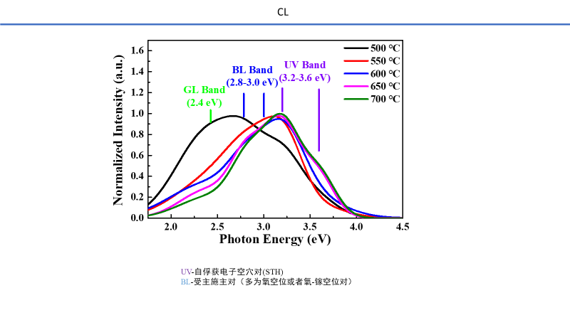
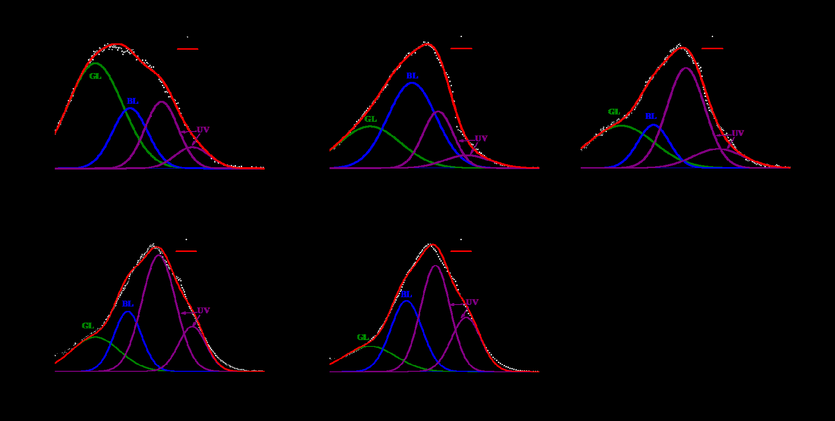
![Figure 5: AFM images of the surface morphology for β-Ga2O3 films deposited at 500, 550, 600, 650 and 700 ℃. And the RMS values of surface roughness of β-Ga2O3 films as a function of substrate temperature. The room-temperature CL results from the β-Ga2O3 thin films are found to be strongly dependent on the substrate temperatures as shown in Figure 6. Three major light emission features are obvious from each spectrum and the energy correspond to 2.4 eV, 2.8-3.0 eV and 3.2- 3.6 eV, named as green luminescence (GL) band, blue luminescence (BL) band and UV band, respectively. The UV band is generally assigned to recombination of free electrons and self-trapped holes [26-28]. And the BL band may result from defect related luminescence, attributed to donor-acceptor pair (DAP) recombination. Possible donors are intrinsic point defects such as oxygen vacancies (Vo) and interstitial Ga (Gai), and possible acceptors are Ga vacancies (VGa), Vo-VGa complexes [26-28]. Thus, the change of CL spectra is considered to be caused by the variation of crystal quality of the β-Ga2O3 thin films. As the substrate temperature increases, the luminescence of BL band and GL band gradually decreases, while the UV band luminescence increases, illustrating the improvement of crystal quality. In order to further quantitatively compare the luminescence ratio, each spectrum is fitted by four peaks, as shown in Figure 7(a)-(e). Note that the UV is fitted by the two peaks because the photogenerated holes can self-trap onto two different O sites [29,30]. Figure 7f shows the summation area of BL an GL peaks with respect to the area of the UV peak as a function of the substrate temperature. The relative intensity ratio of BL and GL to UV decreases with the increasing of substrate temperature, and the ratio reaches the lowest value when the substrate temperature is 700℃. This result implies that among these substrate temperatures, the β-Ga2O3 thin film has the best crystal quality at the substrate temperature of 700℃, which is consistent with the XRD rocking curves as shown in Figure 1b.](/fulltextimages/6797/fig_5.png)
Figure 5: AFM images of the surface morphology for β-Ga2O3 films deposited at 500, 550, 600, 650 and 700 ℃. And the RMS values of surface roughness of β-Ga2O3 films as a function of substrate temperature. The room-temperature CL results from the β-Ga2O3 thin films are found to be strongly dependent on the substrate temperatures as shown in Figure 6. Three major light emission features are obvious from each spectrum and the energy correspond to 2.4 eV, 2.8-3.0 eV and 3.2- 3.6 eV, named as green luminescence (GL) band, blue luminescence (BL) band and UV band, respectively. The UV band is generally assigned to recombination of free electrons and self-trapped holes [26, 27, 28]. And the BL band may result from defect related luminescence, attributed to donor-acceptor pair (DAP) recombination. Possible donors are intrinsic point defects such as oxygen vacancies (Vo) and interstitial Ga (Gai), and possible acceptors are Ga vacancies (VGa), Vo-VGa complexes [26, 27, 28]. Thus, the change of CL spectra is considered to be caused by the variation of crystal quality of the β-Ga2O3 thin films. As the substrate temperature increases, the luminescence of BL band and GL band gradually decreases, while the UV band luminescence increases, illustrating the improvement of crystal quality. In order to further quantitatively compare the luminescence ratio, each spectrum is fitted by four peaks, as shown in Figure 7(a)-(e). Note that the UV is fitted by the two peaks because the photogenerated holes can self-trap onto two different O sites [29, 30]. Figure 7f shows the summation area of BL an GL peaks with respect to the area of the UV peak as a function of the substrate temperature. The relative intensity ratio of BL and GL to UV decreases with the increasing of substrate temperature, and the ratio reaches the lowest value when the substrate temperature is 700℃. This result implies that among these substrate temperatures, the β-Ga2O3 thin film has the best crystal quality at the substrate temperature of 700℃, which is consistent with the XRD rocking curves as shown in Figure 1b.
Conclusion
In conclusion, β-Ga2O3 thin films are grown on c-plane GaN template substrate by ozone MBE. Phase-pure (-201)-oriented β-Ga2O3 thin film can be formed with the substrate temperature exceeded 550 ℃, and the crystal quality improves with increasing substrate temperature. The epitaxial relationships are confirmed as β-Ga2O3 [10] // GaN [11, 12, 13, 14, 15, 16, 17, 18, 19, 20] and β-Ga2O3 [102] // GaN [1, 2, 3, 4, 5, 6, 7, 8, 9, 10, 11, 12, 13, 14, 15, 16, 17, 18, 19, 20, 21, 22, 23, 24, 25, 26, 27, 28, 29, 30, 31, 32, 33, 34, 35, 36, 37, 38, 39, 40, 41, 42, 43, 44, 45, 46, 47, 48, 49, 50, 51, 52, 53, 54, 55, 56, 57, 58, 59, 60, 61, 62, 63, 64, 65, 66, 67, 68, 69, 70, 71, 72, 73, 74, 75, 76, 77, 78, 79, 80, 81, 82, 83, 84, 85, 86, 87, 88, 89, 90, 91, 92, 93, 94, 95, 96, 97, 98, 99, 100], and result six-fold domain structure in β-Ga2O3 thin film. Because the difference in crystal structure between the film and the substrate, the β-Ga2O3 thin film follows the island-growth model, and the size of the island increases as the substrate temperature increases. In addition, CL spectra variations are observed that the defect related luminescence decreases with the increase of substrate temperature, claiming the improvement of crystal quality which are consistent with the results of XRD rocking curves. The presented optimized β-Ga2O3 thin film grown on GaN template substrate should effectively promote development of reliable high performance self-powered UV photodetector based on the Ga2O3/GaN heterojunction.
References
-
Guo D, Guo Q, Chen Z, Wu Z, Li P, et al. (2019) Review of Ga2O3-based optoelectronic devices. Materials Today Physics 11: 100157.
-
Zhou H, Zhang J, Zhang C, Feng Q, Zhao S, et al. (2019) A review of the most recent progresses of state-of-art gallium oxide power devices. Journal of Semiconductors 40: 011803.
-
Stepanov SI, Nikolaev VI, Bougrov VE, Romanov AE (2016) Gallium Oxide: Properties and Applications - A Review. Rev Adv Mater Sci 44: 63-86.
-
Baldini M, Galazka Z, Wagner G (2018) Recent progress in the growth of β-Ga2O3 for power electronics applications. Mater Sci Semicond Process 78: 132-146.
-
Tadjer MJ, Lyons JL, Nepal N, Freitas JA, Koehler AD, et al. (2019) Review-Theory and Characterization of Doping and Defects in β-Ga2O3. ECS Journal of Solid State Science and Technology 8(7): Q3187-Q3194.
-
Chen X, Ren F, Gu S, Ye J (2019) Review of gallium-oxide- based solar-blind ultraviolet photodetectors. Photonics Research, 7(4): 381-415.
-
Fan MM, Lu YJ, Xu KL, Cui YX, Cao L, et al. (2020) Growth and characterization of Sn-doped β-Ga2O3 thin films by chemical vapor deposition using solid powder precursors toward solar-blind ultraviolet photodetection. Appl Surf Sci 509: 144867.
-
Xiao Y, Liu L, Ma ZH, Meng B, Qin SJ, et al. (2019) High- Performance Self-Powered Ultraviolet Photodetector Based on Nano-Porous GaN and CoPc p–n Vertical Heterojunction. Nanomaterials 9(9): 1198.
-
Guo D, Su Y, Shi H, Li P, Zhao N, et al. (2018) Self- Powered Ultraviolet Photodetector with Superhigh Photoresponsivity (3.05 A/W) Based on the GaN/ Sn:Ga2O3 pn Junction. ACS nano 12(12):12827-12835.
-
Li P, Shi H, Chen K, Guo D, Cui W, et al. (2017) Construction of GaN/Ga2O3 p–n junction for an extremely high responsivity self-powered UV photodetector. J Mater Chem C 5(40): 10562-10570.
-
He T, Zhang X, Ding X, Sun C, Zhao Y, et al. (2019) Broadband Ultraviolet Photodetector Based on Vertical Ga2O3/GaN Nanowire Array with High Responsivity. Advanced Optical Materials 7(7): 1801563.
-
Li W, Hu Z, Nomoto K, Zhang Z, Hsu JY, et al. (2018) 1230 V β-Ga2O3 trench Schottky barrier diodes with an ultra-low leakage current of <1 μA/cm2. Appl Phys Lett 113(20): 202101.
-
Lv YJ, Liu HY, Wang YG, Fu XC, Ma CL, et al. (2020) Oxygen annealing impact on β-Ga2O3 MOSFETs: Improved pinch- off characteristic and output power density. Appl Phys Lett 117(13): 133503.
-
Feng ZQ, Tian XS, Li Z, Hu ZZ, Zhang YN, et al. (2020) Normally-Off- β -Ga2O3 Power MOSFET With Ferroelectric Charge Storage Gate Stack Structure. IEEE Electron Device Lett 41(3): 333-336.
-
Chabak KD, McCandless JP, Moser NA, Green AJ, Mahalingam K, et al. (2018) Recessed-Gate Enhancement- Mode β -Ga2O3 MOSFETs. IEEE Electron Device Lett 39(1): 67-70.
-
Feng B, Li Z, Cheng F, Xu L, Liu T, et al. (2020) Investigation of β‐Ga2O3 Film Growth Mechanism on c‐Plane Sapphire Substrate by Ozone Molecular Beam Epitaxy. Physica status solidi (a), pp: 2000457.
-
Qian LX, Wang Y, Wu ZH, Sheng T, Liu XZ (2017) β-Ga2O3 solar-blind deep-ultraviolet photodetector based on annealed sapphire substrate. Vacuum 140: 106-110.
-
Wakabayashi R, Yoshimatsu K, Hattori M, Ohtomo A (2017) Epitaxial structure and electronic property of β-Ga2O3 films grown on MgO (100) substrates by pulsed- laser deposition. Appl Phys Lett 111(16): 162101.
-
Li JS, Zhang XD, Cao X, Xu K, Zhang L, et al. (2020) Self- catalyzed metal organic chemical vapor deposition growth of vertical β-Ga2O3 nanowire arrays. Nanotechnology 31(2): 02LT01.
-
Nakagomi S, Kokubun Y (2016) Crystal orientations of β‐Ga2O3 thin films formed on c‐plane GaN substrate. physica status solidi (b) 253(6): 1217-1221.
-
Wang D, He L, Le Y, Feng X, Luan C, et al. (2020) Characterization of single crystal β-Ga2O3 films grown on SrTiO3 (100) substrates by MOCVD. Ceramics International 46(4): 4568-4572.
-
Wang D, He L, Ma X, Xiao H, Le Y, et al. (2020) Preparation and properties of heteroepitaxial β-Ga2O3 films on KTaO3 (100) substrates by MOCVD. Materials Characterization 165: 110391.
-
Wang Q, Chen J, Huang P, Li M, Lu Y, et al. (2019) Influence of growth temperature on the characteristics of β-Ga2O3 epitaxial films and related solar-blind photodetectors. Appl Surf Sci 489: 101-109.
-
Cao Q, He L, Xiao H, Feng X, Lv Y, et al. (2018) β-Ga2O3 epitaxial films deposited on epi-GaN/sapphire (0001) substrates by MOCVD. Mater Sci Semicond Process 77: 58-63.
-
Vogt P, Bierwagen O (2018) Quantitative subcompound- mediated reaction model for the molecular beam epitaxy of III-VI and IV-VI thin films: Applied to Ga2O3, In2O3, and SnO2. Phys Rev Mater 2(12): 120401.
-
Onuma T, Nakata Y, Sasaki K, Masui T, Yamaguchi T, (2018) Modeling and interpretation of UV and blue luminescence intensity in β-Ga2O3 by silicon and nitrogen doping. J Appl Phys 124(7): 075103.
-
Huynh TT, Lem LLC, Kuramata A, Phillips MR, Ton C (2018) Kinetics of charge carrier recombination in β-Ga2O3 crystals. Phys Rev Mater 2(10): 105203.
-
Gao HT, Muralidharan S, Pronin N, Karim MR, White SM, et al. (2018) Optical signatures of deep level defects in Ga2O3. Appl Phys Lett 112(24): 242102.
-
Wang YS, Dickens PT, Varley JB, Ni XJ, Lotubai E, et al. (2018) Incident wavelength and polarization dependence of spectral shifts in β-Ga2O3 UV photoluminescence. Scientific Reports 8: 180715.
-
Frodason YK, Johansen KM, Vines L, Varley JB (2020) Self- trapped hole and impurity-related broad luminescence in β-Ga2O3. J Appl Phys 127(7): 075701.
- Solution-Processed Chiral Perovskites for Biomedical Applications
- Nanotechnology in Health Chemistry and Medicine: Current Challenges and Future Directions
- Human Exposure to Micro- and Nanoplastics: Pathways, Toxicity, and Intervention Strategies
- Exosome Nanomedicine for Cancer Therapy
- Micro and Nanoplastics–Plastisphere, Biotoxicity, Impact on Human Health, and Mitigation Strategies
- Process Validation of Cefixime Powder for Suspension Dosage Form, 50 mL