Laser Based Multi-Quantum Wells
The basic advantage of using multiple quantum wells (MQWs) in a laser system is that the threshold current density is reduced relative to conventional lasers due to the increased carrier density in MQWs and the associated increase in the optical gain due to the huge confinement factor. The temperature sensitivity of this gain is also reduced compared to bulk material so that the MQWs-based laser can be designed to operate efficiently at room temperature much higher than conventional semiconductor lasers.
Abbreviation
MQW: Multiple Quantum Wells.
Introduction
Multi-Quantum Well (MQWs) structures were first proposed by Esaki and Tsu in 1970 to be explored in many opto-electronic areas. The MQWs are formed by using alternate thin layers of two different direct band gap semiconductors. When the layer thickness is made lesser than the de-Broglie wavelength of the charge carriers (generally 10-20nm), it is said to be a quantum well. The electrons and holes in the MQW are confined in 1-dimension thus getting discrete energy levels. This is an analogy to the discrete energy levels of electrons in an atom. Now if the width of the well is varied, it is possible to get specific energy level for the particles, thus making the band gap of the material adjustable. This has a insightful impact on the optical and electrical properties of the material. Laser is an acronym for Light Amplification by Stimulated Emission of Radiation which was first proposed by Einstein in 1917. This can be understood by referring to Figure 1, in which a charged particle emits photons when falling from a higher energy level to a lower one. In Figure 1, where the particle is near other atoms, the photon emitted can strike the other atoms making the particle fall further and result in emitting more photons. This is the process of stimulated emission. In order to achieve laser operation, it is necessary to have more atoms in higher energy levels than lower ones which can be done by the process called population inversion, in which the atoms are pumped to high energy levels using an external energy source, and then allowed to relax and give the stimulated emission. A large number of atoms emitting photons randomly in phase can result in high-intensity laser.
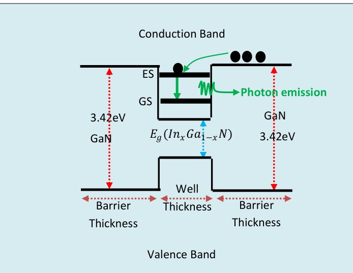
Figure 1 represents the schematic diagram of the single QW-based laser showing the ground, excited and reservoir states. The main parameters governing the MQWs-based laser characteristics are the chemical content and size of the Well/Barrier. The band gap energy of the ternary (In,Ga)N which depend nonlinearly on the In-content is expressed as follows:
$$E_g(\text{In}_x\text{Ga}_{1-x}\text{N}) = xE_g(\text{InN}) + (1-x)E_g(\text{GaN}) - 1.43x(1-x)$$
Quantum cascade (QC) lasers are electrically injected laser consisting of a semiconductor heterostructure. These are so-called intersubband or unipolar laser because their operation is based on the radiative emission of electrons between confined levels in the conduction band of MQWs structure. The physical phenomenon responsible for the radiative emission therefore differs from that used in laser diodes since the latter is not due to the recombination between electrons from the conduction band and holes in the valence band, but is due to the deexcitation (relaxation) of carriers between two subbands of the conduction band. The carrier confined energies are obtained from the Poisson- Schrodinger coupling equation given as:
H E
$$ \left\{ \begin{array}{l} H \Psi = E \Psi \\ \vec {\nabla}. \vec {D} = \rho \end{array} \right. $$ .
D ρ
Where, H is the carrier’s Hamiltonian, E is the carrier’s energy, Ψ is the carrier’s wave function, D ⃗ is the electric displacement field and ρ is the carrie’s charge density.
In this case, the transition’s energy (
) ES GS E E − depends
strongly on the thickness of the wells and barriers on the
one hand and the chemical Indium content (
$$ \left( \operatorname {I n} _ {x} G a _ {1 - x} N \right) \mathrm {o n} $$
the other hand. This particularity allows QC lasers achieve
energies previously inaccessible for laser diodes and offer
great flexibility in the choice of wavelength. As an example,
we can cite QC lasers based of InGaAs/AlInAs since they cover the spectral range between λ ≥ 3.4 μm [1] and λ ≤ 24 μm [2] and even the terahertz [3]. It is for this reason that they are a very suitable for spectroscopic analysis systems, particularly for the detection of trace gases [4].
QC lasers have experienced very rapid development since their first demonstration in 1994 [5]. The first device was epitaxially grown based on InGaAs/InAlAs/InP materials and emitted at λ = 4.2 μm working in pulsed regime up to 88 K but required high threshold current density (
$$ \left(1 4 k A. c m ^ {- 2}\right). $$
Since then, the quality and performance of these lasers have
only improved. Today they cover a wide spectral range in the mid-infrared (
$$ \left(2. 7 5 \mu m \leq \lambda \leq 2 4 \mu m\right) 。 $$
and in the terahertz
$$ \left(6 0 \mu m \leq \lambda \leq 2 5 0 \mu m\right). $$
. They operate at 298K [6, 7], in
continuous mode [8, 9] reaching powers up to 1.3 W with a
threshold current density as low as
2 1.7 . kA cm − [10]. These improvements have emerged at the cost of considerable efforts in the:
- Optimization of epitaxy techniques,
- Design of band structures of heterostructures,
- Optimization of optical confinement, To reach small wavelengths, researchers focused on Antimonide (Sb) materials showing high band offset discontinuities (Table 1). Devenson et al. increased the emission of InAs/AlSb quantum cascade lasers at λ ≅ 2.75 μm [11] and achieved spontaneous intersubband emission at λ ≅ 2.55 μm [12]. The InGaAs/AlAsSb pair on an InP substrate effectively covers the surrounding window (
$$ \left(3 \mu m < \lambda \leq 5 \mu m\right) $$
. In 2007, Revin et al. showed a cascade laser that emits at 3
μm and works in a pulsed mode at room temperature [13]. To
create laser capable of operating at telecom wavelengths (1.3
μm ≤ λ < 1.55 μm), materials having a broad band offset, such
as nitrides, are in the viewpoint.
| Well/Barrier | Substrat | Band offset (eV) |
|---|---|---|
| InAS/AlSb | InAs or GaSb | 2.1 |
| In$_{0.53}$Ga$_{0.47}$As/AlAs$_{0.56}$Sb$_{0.44}$ | InP | 1.6 |
| In$_{0.53}$Ga$_{0.47}$As/Al$_{0.48}$In$_{0.52}$As | InP | 0.52 |
| GaAs/AlxGaxAs | GaAs | Adjustable |
Table 1: The Conduction Band Offset Discontinuity in Different Materials Used for QC Laser Manufacturing.
For instance, due to their exceptional optical and electrical properties, tunable band gap energies, thermal and chemical stabilities and high conduction band off-set, alloys like (In,Ga)N have recently attracted attention [14, 15, 16, 17, 18, 19, 20, 21, 22]. The MQW lasers have shown that they can have a current density threshold 1kA/cm-2 for a wavelength equals to 1.3µm. The most promising cost saving application in the field of telecommunications is the use of MQWs in the transmission of voice and data. By using MQWs it is possible to build an electrically pumped laser source at 1.3µm. Currently, the most widely used source is the light emitting diode. Unfortunately, the LED is a non-coherent source and suffers from large modal dispersion in optical fibre. An external cavity laser can be coated to provide single mode operation but these devices are very costly mainly because of the excessive number of processes needed to build a V-groove diffraction grating. It is not unexpected that mQWs lasers have been dubbed “the ideal material for the information age” because of these qualities, which make them particularly appealing for a variety of applications such as:
- Optical fiber communications
- Optical data storage,
- Medicine,
- Military, However, the MQWs-based lasers face several limitations and challenges such as:
- Fabrication complexity: MQW structure manufacturing involves careful control of layer thickness and composition of materials, which renders it more difficult and costly.
- Thermal impacts: MQW lasers are subject to temperature fluctuations which can diminish effectiveness and cause wavelength shifts.
- Carrier leakage: At high temperatures and/or inject levels, carriers may migrate from well layers and penetrate the barrier ones, limiting laser performance.
- Strain and defects: Mismatches in lattice constants between Quantum wells and barrier materials can generate strain, resulting in defects and dislocations that degrade effectiveness and endurance.
- Aging and reliability: MQW lasers may gradually degrade over time owing to defects in the layers or material interfaces, reducing their lifetime and stability.
Conclusion and Perspective
In summary, a brief overview in the area of laser-based on different material and the perspective of the III-nitride semiconductors has been covered in this work. Because of their direct and adjustable band gap and great dependability, III-nitride semiconductors are an excellent choice for a wide range of electrical and optoelectronic applications, including high efficiency laser diodes, solar cells and brilliant LEDs. The functionality and dependability of the final device are impacted by a multitude of critical material qualities that are determined by the substrate selection. Integrating InGaN- based material, with currently available laser like AlSb, GaAs- based, is the best solution in order to get efficiencies greater than achieved results.
References
-
Faist J, Capasso F, Sivco DL, Hutchinson AL, Chu SNG, et al. (1998) Short wavelength (λ = 3.4 μm) quantum cascade laser based on strained compensated InGaAs/ AlInAs. Applied Physics Letters 72(6): 680-682.
-
Colombelli R, Capasso F, Gmachl C, Hutchinson AL, Sivco DL, et al. (2001) Far-infrared surface-plasmon quantum- cascade lasers at 21.5 μm and 24 μm wavelengths. Applied Physics Letters 78(18): 2620–2622.
-
Ajili L, Scalari G, Hoyler N, Giovannini M, Faist J (2005) InGaAs-AlInAs/InP terahertz quantum cascade laser. Applied Physics Letters 87(14): 141107
-
Tittel FK, Bakhirkin Y, Kosterev AA, Wysocki G (2006) Recent Advances in Trace Gas Detection Using Quantum and Interband Cascade Lasers. The Review of Laser Engineering 34(4): 275.
-
Faist J, Capasso F, Sivco DL, Hutchinson AL, Cho AY (1994) Second and third harmonics generation by coherent sub- THz radiation at induced Lifshitz transitions in gapped bilayer grapheme. Quantum Cascade Laser Science 264: 553.
-
Teissier R, Barate D, Vicet A, Alibert C, Baranov AN (2004) Room temperature operation of InAs/AlSb quantum cascade lasers. Applied Physics Letters 85(2): 167-169.
-
Faist J, Sirtori C, Capasso F, Sivco DL, Baillargeon JN, et al. (1988) High-power long-wavelength (λ = 11.5 μm) quantum cascade lasers operating above room temperature. Photonics Technology Letters IEEE 10: 1100-1102.
-
Evans A, Yu JS, Slivken S, Razeghi M (2004) High- temperature, high-power, continuous-wave operation of buried heterostructure quantum-cascade lasers, Applied Physics Letters 84(3): 314-316.
-
Yu JS, Slivken S, Evans A, Darvish SR, Nguyen J, et al. (2006) High power λ ≃ 9.5 μm quantum-cascade lasers operating above room temperature in continuous-wave mode. Applied Physics Letters 88(9) :91113.
-
Bai Y, Darvish SR, Slivken S, Zhang W, Evans A, et al. (2008) Room temperature continuous wave operation of quantum cascade lasers with watt-level optical power. Applied Physics Letters 92(10): 101105.
-
Devenson J, Cathabard O, Teissier R, Baranov AN (2007) InAs/AlSb quantum cascade lasers emitting at 2.75-2.97 μm, Applied Physics Letters 91(25): 251102.
-
Barate D, Teissier R, Wang Y, Baranov AN (2005) Short wavelength intersubband emission from InAs/AlSb quantum cascade structures. Applied Physics Letters 87(5): 051103.
-
Revin DG, Cockburn JW, Steer MJ, Airey RJ, Hopkinson M, et al. (2007) InGaAs/AlAsSb/InP quantum cascade lasers operating at wavelengths close to 3 μm. Applied Physics Letters 90: 21108.
-
Ghazi HE, En-Nadir R, Jorio A, Zorkani I (2021) Ground- state Shallow-donor Binding Energy in (In,Ga)N/GaN Double QWs Under Temperature, Size, and the Impurity Position Effects. J Model Simul Mat 4(1): 1-6.
-
Abboudi H, Ghazi HE, Benhaddou F, Nadir RE, Jorio A, et al. (2022) Temperature-related photovoltaic characteristics of (In,Ga)N single-intermediate band quantum well solar cells for different shapes. Physica B Condensed Matter 626: 413495.
-
Abboudi H, Ghazi HE, En-nadir R, Basyoon-Kabatas MA, Jorio A, et al. (2024) Efficiency of InN/InGaN/ GaN Intermediate-Band Solar Cell under the Effects of Hydrostatic Pressure, In-Compositions, Built-in-Electric Field, Confinement, and Thickness. Nanomaterials 14(1): 104.
-
En-nadir R, Ghazi HE, Jorio A, Zorkani I, Kiliç HS (2022) Intersubband optical absorption in (In,Ga)N/GaN double quantum wells considering applied electric field effects. J Comput Electron 21: 111-118.
-
En-nadir R, Kabatas MAB, Tihtih M, Belaid W, Ez-zejjari I, et al. (2023) Enhancing Emission via Radiative Lifetime Manipulation in Ultrathin InGaN/GaN Quantum Wells: The Effects of Simultaneous Electric and Magnetic Fields, Thickness, and Impurity. Nanomaterials 13(21): 2817.
-
En-nadir R, El-ghazi H, Leontie L, Tihtih M, Zaki SE, et al. (2023) Tailoring optoelectronic properties of InGaN-based quantum wells through electric field, indium content, and confinement shape: A theoretical investigation. Physica B Condensed Matter 663: 414976.
-
Ghazi HE, Jorio A (2013) Excited-states of hydrogenic- like impurities in InGaN–GaN spherical QD: electric field effect. Physica B Condensed Matter 430: 81-83.
-
En-nadir R, Ghazi H, Belaid W, Jorio A, Zorkani I, et al. (2021) Ground and first five low-lying excited states related optical absorption in In.1Ga.9N/GaN double quantum wells: Temperature and coupling impacts. Solid State Communications 338: 114464.
-
En-nadir R, Ghazi HE, Jorio A, Zorkani I (2021) Ground- state Shallow-donor Binding Energy in (In,Ga)N/GaN Double QWs Under Temperature, Size, and the Impurity Position Effects. J Mod Sim Mater 4(1): 1-6.
- Solution-Processed Chiral Perovskites for Biomedical Applications
- Nanotechnology in Health Chemistry and Medicine: Current Challenges and Future Directions
- Human Exposure to Micro- and Nanoplastics: Pathways, Toxicity, and Intervention Strategies
- Exosome Nanomedicine for Cancer Therapy
- Micro and Nanoplastics–Plastisphere, Biotoxicity, Impact on Human Health, and Mitigation Strategies
- Process Validation of Cefixime Powder for Suspension Dosage Form, 50 mL