Analysis of Bulk and Surface Radiation Damage in n+ in p SFz Si Micro Strip Detectors for the Future High Luminosity Collider Experiments: TCAD Simulation and Measurements
Within the framework of CERN RD50 collaboration, several radiation damage models for n/p-SFz, n-MCz Si have been explored for the better understanding of the experimental results in radiation damage analysis of the irradiated Si detectors. In the present paper, the important review on the microscopic radiation damage model for the p-type SFz Si detector combining the surface and radiation damage effects that can be used to simulate radiation damages effects in the heavily irradiated detectors for the good comparison of the experimental data and simulation result. The surface radiation damage models were extracted from the experimental measurements on the p-MOS capacitor and Gate-Controlled Diodes irradiated by Gamma or X-ray radiations in the range of 10 to 500 Mrad (Si). Whereas, the bulk damage model microscopic parameter was extracted from the experimental (TSC, DLTS) measurements on the n in p-SFz Si microstrip detector. The radiation damage (surface and bulk) models can be fed into the commercial Synopsys TCAD device simulator program for the designing and optimization of the detector, which can be used in the very harsh radiation environment of the HL-LHC, or FCC experiment. The objective of this analysis was to verify the experimental results using the new microscopic radiation damage models on the p-SFz Si for the radiation damage analysis of p- SFz Si detectors irradiated by proton, neutron or mixed at very high fluences. The results were verified by comparison of the experimental data with TCAD simulation.
Srivastava Ajay K*, Deepali and Patyal S
Introduction
The LHC (Large Hadron Collider) will be upgraded to HL (High Luminosity)-LHC in 2026 and will be assume a luminosity of 7.5 x 1034 cm-2) so it will require a new radiation hard solid state detectors for the new CMS tracker detector upgrade for the outer tracking area [1]. Within CERN RD50 collaboration, p-type detector was identified as a suitable device for the HL-LHC and Future Circular Collider (FCC)
experiments, due to its higher Charge Collection Efficiency (CCE) [2]. The choice of the detector material SFz (Standard Float Zone) /MCz (Magnetic Czochralski) is a questionable and a lot of research and research is needed to investigate the macroscopic performance of the detector for the future colliders. Therefore, it is imperative to design and optimize a thin n in p (SFz/MCz) Si micro strip detector for the long- term performance of the detectors at high luminosity collider experiments.
The radiation damage reduces the electrical performance of the Si detector in hostile radiation environment of the experiments. The radiation damage can be divided into two groups: 1) Bulk damage 2) Surface damage [3, 4, 5]. Bulk damage introduces an acceptor, and donor-type deep traps in the Si material, and this can change the macroscopic properties of the detector. At very high FCC fluence of the order of 1 x 10¹⁷ /cm2 (Equivalent to 1 MeV neutron), it might give a very high leakage current, more than 1000V full depletion voltage, and CCE degradation occurs in the detector. These deep traps depend on the material of the substrate (SFz/MCz), and the type of detector; it is an n type or p type Si substrate. Surface damage introduces the localized oxide charges at the interface, which affects the avalanche breakdown voltage, interstrip or interpixel capacitance, and charge collection properties of irradiated silicon detectors [6]. A number of radiation damage models have been developed to simulate the radiation damage effects in n / p Si micro strip detectors at the fluence of the order of 1016/cm2, but due to the lack of the experimental data at FCC fluences, it is difficult to compare the TCAD simulation data’s with the experimental data. In this review paper, a few of good experimental data and simulated results on heavily irradiated n in p SFz Si detector combining surface and bulk radiation damage effects are discussed in detail for the designing to start a silicon microstrip detector for the FCC.
TCAD Device and Process Simulation Technique
TCAD device and process simulators are used since last 30 years to analyze the performance of the semiconductor devices. TCAD has shown interest in the radiation detector community because it is an inexpensive way to design a radiation -resistant Si detector for the harsh radiation environment of the HL-LHC, or FCC. The flexibility of choosing correct physical models in the TCAD device simulation program makes the real analysis of the non-irradiated and irradiated Si detectors, and as a result, the simulation results can be compared with the experimental data’s [5].
The TCAD process simulation uses the semiconductor radiation detector processing steps. These processing steps are oxidation, etching (dry/wet), ion implantation, and high/ low temperature annealing, which can be obtained from the foundry for the fabrication of detectors. This process simulator generates an output file, which can be used as an input file to the device simulator. By solving these equations are such as: Poisson equation, current continuity equations of Jn (n, p) and Jp (n, p), drift-diffusion equation and heat conduction equations, which is a function of TL, where n, p, TL stands for electrons, holes and lattice temperature simultaneously. The device simulators integrated semiconductor physics for the transport, mobility, generation-recombination Shockley-Read-Hall, auger, impact ionization, deep trap, and surface interface trap, fixed oxide charge etc. this was done by using default models and their parameters listed in the TCAD device simulator. Some of physical models are needed to use to reproduce the experimental results on the irradiated Si detectors are Hurkx Trap Assisted Tunneling, Van Overstraeten-De avalanche model. Van Overstraeten- De avalanche Model is used for the “avalanche multiplication” effect this is because of the impact ionization that occurs at a very bias voltage in the irradiated detector.
Radiation Damage Model for SFz Si Detector
Within CERN RD50 collaboration, a few of detector groups have developed two/three deep traps radiation damage model for n and p type semiconductor (SFz) material. For the most SFz (Si) detectors, the model shows a good comparison of the experimental and simulated result for the fluence of 1x10¹⁵ neq./cm2 1MeV equivalent neutrons [7]. Srivastava AK [5] developed the n-MCz neutron irradiated four level deep trap model that can be used to simulate the macroscopic effects of radiation damage up to 8x10¹⁴ neq. / cm2 [5].
The Si detector irradiated with very high fluences can be simulated combining bulk and surface radiation damage model [7]. Here, the p-type deep trap model for SFz Si, which was, used in the TCAD device simulation for the radiation damage effects in the n in p SFz Si detectors. It shows a very good comparison between the experimental data and simulation results. This p-type deep trap model for SFz Si can be also used to investigate the radiation damage effects in the p- SFz Si detector for the new upgrade of the CMS tracking detector at HL-LHC in 2026, and also for the FCC. The p-MCz Si four level deep traps mixed irradiation model is being developed for the development of detectors for the FCC [8]. Figure 1 shows the simulated the flux level in CMS Tracker after 3000 fb-1.
![Figure 1: FLUKA simulated the flux level in CMS Tracker after 3000 fb-1. The Z coordinate in the legend indicates the distance from the collision point along the ray line [1].](/fulltextimages/9776/fig_1.png)
Experimental Measurements
The current/voltage (I/V) and (C/V) capacitance/voltage measurements are used to measure the generation leakage current and full depletion voltage (Vfd) at room temperature of 200C and after the beneficial annealing of 80°C for 10 min in heavily irradiated Si detectors. The Thermally Stimulated Current (TSC) and Deep Level Transient Spectroscopy (DLTS) measurement gives the information about the microscopic deep-trap defects in the irradiated Si detectors. The test structures; gate-controlled diodes, p-Metal Oxide capacitor can be irradiated by gamma rays between 10Mrad (Si)-500Mrad (Si), or by 10 kV x-rays for the interfacial study in x-ray or gamma-ray irradiated detectors. The interfacial properties of SiO2 layer and Si-SiO2 interface were studied using the C/V technique, Thermally Depolarization Technique (TDRC) techniques. The microscopic parameters are extracted from the measurements; Nfix (oxide charge density), interfacial trap density (N in cm-2 or D in cm- 2eV-1) and traps (donor/acceptor) type can be extracted.
The microscopic model parameters can be fed into the TCAD device simulation for the surface radiation damage study [9]. Nfix was order of 2×1010 cm-2 in <100>SFz Si wafer before irradiation. It was found after 10 Mrad (Si) dose, Nfix ox decreases with an increases doses; Nfix ox at this dose was 0.8×1012 cm-2 Interface traps density was an order of 109 -1010 cm-2eV-1 from valence band edge range of 0.2 eV to 0.6 eV. The reason is not still clear yet, why there is decrease of the fixed oxide charges at higher doses of 10 Mrad (Si).
The similar investigations have been observed in the development of the Adaptive Gain Integrating Pixel Detector (AGIPD) detector for the Eu X-Ray Free Electron Laser (EuXFEL) at DESY, Hamburg, Germany. Here, we were proposed the surface damage model for surface damage effects using experimental data’s; two-interface trap model and x ray damage parameter for the different x-ray doses that was implemented into TCAD device simulation program [5, 9, 10, 11, 12] (Table 1). Table 1 shows the surface damage model for the detector irradiated by 10 keV x-rays.
| S.No. | Interface defects | Levels (eV) | Defects concentration |
|---|---|---|---|
| 1 | Acceptor | E-0.4 c | 40% of acceptor N (N =0.8 Nfix ) it it ox |
| 2 | Acceptor | E-0.6 c | 60% of acceptor N (N =0.8 Nfix ) it it ox |
| 3 | Donor | E+0.6 v | 100% of acceptor N (N =0.8 Nfix ) it it ox |
Table 1: Surface damage model for the detector irradiated by 10 keV x-rays [10]. The capture cross- sections for all defects = 1×
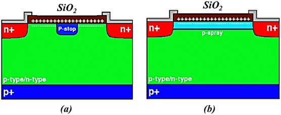
Technology Evolution of Isolation Technologies in N+P Si Microstrip Detector
The n+p-p+ Si microstrip detector model is using p-spray or p-stop strip isolation technology. An isolation technology is used to protect the n+ in p Si detector from the shortening of the n+ microstrips, which can be due to an accumulation layer of electrons formed due to the fixed oxide charge in the oxide just, which is below at an interface of Si-SiO2. The p-implantation is done by two methods between two n+- implants, which are p-stop and p-spray. These technologies with suitable p-stop/p-spray doses and depth can reduce the electric field at n+ edge of the implant layer in the silicon n+p microstrip detector, which can results the protection of the detector from the premature breakdown voltage of the detector, and it can increase the charge collection too in the irradiated detector. Figure 2 shows (a) p-stop and (b) p-spray strip isolation model in the n+p-p+ Si detector.
Microscopic Surface Radiation and Bulk Damage Model for P-Type Si Bulk
The surface damage introduces microscopic defects at Si-SiO2 interface in the x-ray or gamma ray irradiated detector. Whereas the bulk damage gives the deep-traps in the bulk of Si, and it plays an important role in the electrical characteristics of the Si detector irradiated by very high fluences. The accurate estimation of the capture cross- sections and introduction rates of the different deep traps in the irradiated detectors made of different Si material (SFz, MCz) are not an easy task* [Private communication with Dr. E. Fretwurst]. Finally, the microscopic parameters are required to tune get a good comparison between the experimental data’s and the TCAD simulation results. Table 2 shows the three deep trap radiations damage model for p-type SFz Si bulk [7]. It was also observed that this model can be used up to 7x10¹⁵ n/cm2 to increase the effect of radiation damage in the irradiation Si detector.
| Type | Energy Level (eV) | Capture Cross- Section of Electron ó (Cm-2) e | Capture Cross- Section of Hole ó (Cm-2) h | Introduction Rate ç (Cm-1) |
|---|---|---|---|---|
| Acceptor | E-0.42 eV c | 1x10-15 | 1x10-14 | 1.613 |
| Acceptor | E-0.46 eV c | 7x10-15 | 7x10-14 | 0.9 |
| Donor | Ev+0.36 eV | 3.23x10⁻¹⁵ | 3.23x10⁻¹⁴ | 0.9 |
Table 2: The three deep trap for p-type SFz Si radiation damage model (verified up to 7x 10¹⁵ neq./cm2) [7].
Shockley-Read-Hall recombination statistics can be used determine the effective doping concentration and leakage current in irradiated Si detectors, the equations are [5];
donor acceptor eff D T T N N n n = + − ∑ ∑ , (1)
e n N e e = + (2)
, , , p n donor acceptor donor acceptor T T p n Where ND, giving the initial n-doping concentration, nT (donor, acceptor) represents the defect levels steady state occupancy, NT is the defect concentration and ep,n which is the emission rate for holes and electrons.
The reverse current at Vfd is given by [5];
n I V q Ad e n e n q Ad τ = + ≈ ∑ ∑ (3)
( ) ( ) acceptor donor i fd o n T p T o g eff ,
Where q0 is an elementary charge, area (A), thickness of the sensor is d, carrier concentration (ni), and τg,eff is effective generation lifetime.
Comparison of Experimental Data’s and Simulation Results
The Vfd in 280 μm thick p SFz Si PAD detector is showed up to a fluence of 7x1014 cm-2 are shown in Figure 3. The detector is simulated using the microscopic parameters given in Table 2 for the good comparison of the experimental data’s and simulation results. Here, the C/V measurements were used to determine the Vfd of irradiated Si detectors at room temperature. In heavily irradiated detectors, the back-plane capacitance was not constant at Vfd in the C/V plot, although there is a kink point that has some degree of uncertainty. From the log C-log V plot, the Vfd can be extracted as two straight lines cut each other in the plot [12]. A very good agreement is observed between the experimental data and simulated Vfd up to the fluence of 7x 10¹⁴ neq/cm2 [12, 13]. The uncertainties in Vfd in experimental results on irradiated detectors were taken up to ± 10%, and ±2%. in simulated Vfd.
![Figure 3: The detector is simulated using the microscopic parameters given in Table 2 for the good comparison of the experimental data’s and simulation results. Here, the C/V measurements were used to determine the Vfd of irradiated Si detectors at room temperature. In heavily irradiated detectors, the back-plane capacitance was not constant at Vfd in the C/V plot, although there is a kink point that has some degree of uncertainty. From the log C-log V plot, the Vfd can be extracted as two straight lines cut each other in the plot [12]. A very good agreement is observed between the experimental data and simulated Vfd up to the fluence of 7x 10¹⁴ neq/cm2 [12,13]. The uncertainties in Vfd in experimental results on irradiated detectors were taken up to ± 10%, and ±2%. in simulated Vfd.](/fulltextimages/9776/fig_3.png)
Figure 4 shows the charge collection behavior in 300 micron irradiated n+p Si Microstrip detector at -300C up to a fluence of 2.2 x 10¹⁶ neq. cm-2. The CCE is evaluated by assuming a Minimum Ionizing Particle (MIP) hitting the n+p Si detector perpendicularly to the front side n+ contact. The MIP can be implemented into TCAD device simulation as a heavy ion model that can produce the 80 e-h/micron charges. The accumulated charges were obtained by combining over 20 ns current after subtracting the generation leakage current in Vfd to find the total charge accumulated in the detector on reading electrode. A very good agreement in experimental results and TCAD simulation results in the irradiated p-SFz Si detectors are observed using the surface and bulk damage models (Table 1 and 2). Therefore, p-SFz Si radiation damage model can be also used too for the designing and optimization of the new radiation hard p-SFz Si micro strip detectors for the FCC.
![Figure 4: CCE experimental and simulation data’s (bulk, bulk+surface) in n-in-p Si micro strip irradiated detectors at -300C and 900 V reverse bias [7].](/fulltextimages/9776/fig_4.png)
Figure 5 shows the AC coupled n+ p- SFz Si microstrip design equipped with multiple guard ring, without metal overhang and n+ implant at edge side of the detector/scribe line [6]. In device simulations of non-irradiated detector (for an oxide charge of 4 011 cm-2), it was shown that optimal guard rings without field plates can withstand a reverse voltages above 1000 V .
A breakdown voltage higher than 900 V can be achieved, assuming a fixed oxide charge of 1 1012 cm-2, with the field plates directed toward the active area after exposure to radiation fluence of 1 x 10¹⁵ neq./cm2 [14]. For the higher fluences > 1 x 10¹⁵-17 neq./cm2 at FCC, the design should be study in detail using microscopic radiation damage models combing surface and bulk radiation damage effects in the TCAD device simulation for the different materials for the long term operation of the experiments.
![Figure 5: Cross-section of a AC coupled n+ p- SFz Si microstrip detector equipped with guard ring structure [6].](/fulltextimages/9776/fig_5.png)
Conclusion
For the design and developments of the heavily irradiated advanced Si radiation detectors for the FCC, a new combine surface and bulk radiation damage modeling is discussed. The microscopic surface damage (Nox fix, and Nit) parameters were taken from the measurements on the irradiated p-type substrate test structures MOS capacitor, GCD after gamma radiations in the range of 10-500 Mrad (Si). Whereas, bulk damage parameters have been obtained from the I/-V, C/V, and Thermally Stimulated current measurements. Finally, the modeling of n in p-SFz Si Microstrip detector using TCAD device simulator was able to reproduce the experimental results on the Vfd and CCE in irradiated detectors up to the fluences of the order of 2.2.x1016 neq./cm2. As noted within the CERN RD50 collaborations, n/p MCz is a prime candidate for the detectors reported for the high luminosity collider experiments. So it is imperative to extend this study on this material based detector too for the higher extrapolated (protons/mixed of protons and neutrons) fluences for the FCC.
References
-
Dierlamm A (2019) The CMS Outer Tracker Upgrade for the HL-LHC. Nuclear Instruments and Methods in Physics Research Section A: Accelerators, Spectrometers, Detectors and Associated Equipment 924: 256-261.
-
Moll M (2018) Displacement damage in silicon detectors for high energy physics. IEEE Trans Nucl Sci 65: 1561- 1582.
-
Hartmann F (2017) Evolution of Silicon Sensor Technology in Particle Physics, 2nd(Edn.), Springer Cham, New York, pp: 372.
-
Lutz G (1999) Semiconductor Radiation Detectors, 1st(Edn.), Springer Berlin, Heidelberg, pp: 353.
-
Srivastava AK (2019) Si detector for HEP and photon science experiments: How to design by TCAD simulation. 1st (Edn.), Springer Cham, pp: 183.
-
Dalal A, Bhardwaj R, Ranjan K, Moll M, Peisert EA (2014) Combined effect of bulk and surface damage on strip insulation properties of proton irradiated n+p silicon strip sensors. Journal of Instr 9: P04007.
-
Moscatelli F, Passeri D, Morozzi A, Mendicino R, Betta GFD, et al. (2016) Combined Bulk and surface Radiation Damage Effects at Very High Fluences in Silicon Detectors: Measurements and TCAD Simulations. IEEE Transactions on Nuclear Science 63(5): 2716-2723.
-
Patyal S, Saini N, Kaur B, Chatterjee P, Srivastava AK (2022) Investigation of Mixed Irradiation Effects in p-MCz Thin Silicon Microstrip Detector for the HL-LHC Experiments. Journal of Instrumentation 17: C09023.
-
Schwandt J (2014) Design of a Radiation Hard Silicon Pixel Sensor for X-ray Science. Ph.D. dissertation, Universität Hamburg, Hamburg, Germany, pp: 1-190.
-
Zhang J (2013) X-ray radiation damage studies and design of a silicon pixel sensor for science at the XFEL. Ph.D. dissertation, Universität Hamburg, Hamburg, Germany, 44(31): 1-209.
-
Chilingarov A (2004) Recommendations towards a standardisation of the macroscopic parameter measurements. RD50 Technical Note RD50-2003-03.
-
Lozano M, Pellegrini G, Fleta C, Loderer C, Rafi JM, et al. (2005) Comparision of Radiation Hardness of P-in-N, N-in-N, and N -in-P Silicon Pad Detectors. IEEE Trans Nucl Sci NS-52(5): 1468-1473.
-
Allport P (2019) Applications of silicon strip and pixel -based particle tracking detectors. Nature Reviews Physics 1(9): 567-576.
-
Koyabasi O, Bolla G, Bortoletto D (2010) Guard Ring Simulations for n-on-p Silicon Particle Detectors. IEEE Transactions on Nuclear Science 57(5): 2978-2986.
- Sense, Gravity, Parity & Chirality in Mathematical Physics
- Quantum Lattice Simulations PHYSICS: Microcircuit Particle Formation and Observable Macroscopic Irreversible Time - A Discrete Lagrangian with Cellular Automata Framework
- Quantum Biology from Biomacromolecule to Cell, and Central Dogma Described by Quantum Theory
- Focus, Agility, Speed and Technology (FAST) for Sustainability and Growth
- Square Root Metric Geometry and Pati-Salam Model in Curved Space-Time
- A Simple System Demonstrating the Mpemba Effect in Classical Mechanics