Graphene-Quantum Dots Hybrid Based Dual Band Photodetector
Graphene, which can detect a broad spectrum from ultraviolet to terahertz, is a promising photodetector material because it offers a broad spectral bandwidth and fast response times. However, the nature of weak light absorption has limited the responsivity of graphene-based photodetectors. Here, we demonstrate a responsivity of up to ∼6.7×10³ A/W in a hybrid photodetector that consists of monolayer or bilayer graphene covered with a thin film of colloidal quantum dots. At the same time, benefits from gate-tunability, the device can response from the short-wavelength infrared to the visible, and compatibility with current circuit technologies.
Introduction
Photodetectors (PDs) play an important role in modern society, which convert light into electrical signals [1, 2, 3, 4]. PDs are applied to extremely wide range of applications, including imaging [5], security [6] and optical communication [7]. Although commercial photodetectors based have been widely used, traditional semiconductor materials, such as HgCdTe and InSb, they have limited absorption bands and absorption coefficients [8]. Compared to traditional semiconductor materials, 2D materials are considered to be the most promising materials for photodetectors due to their unique optical and electrical properties [9]. Graphene, one of the most popular two-dimensional materials, interacts strongly with light, with ultrahigh carrier mobility (up to 60,000 cm2 V-1s-1 on a substrate and at room temperature [10]) and no dangling bonds on the surface. For monolayer graphene (thickness about 0.335 nm), the optical absorption coefficient is 2.3% in a wide wavelength range that results the low photoresponsivity [11]. In order to improve the optical absorption of graphene, graphene has been integrated into microcavity [12], waveguide [13] and plasmon resonator [6, 14, 15] to enhance the light-graphene interaction. Graphene/quantum dots hybrid photodetectors have shown ultra-high responsivity up to 108 A/W, which relies on a highly absorbing layer in close proximity to graphene [16]. The absorbing layer induces a shift of the graphene chemical potential upon absorption, hence modifying its channel resistance. Here, based on graphene-quantum structure, we realized the detection of visible to the short-wavelength infrared.
Results and Discussion
The graphene/quantum dots hybrid photodetector we proposed is illustrated in Figure 1(a). By using standard mechanical exfoliation process, single layer graphene is prepared of graphite with tape, then deposited on a Si/SiO2 (285 nm) wafer. And Ni/Au electrodes were fabricated by magnetron sputtering, which defined as the source and n is the carrier concentration and CBG is the geometric capacitance. The FET we fabricated is shown in Figure 1(b). After fabricating graphene FET, the PbS quantum dots (QDs) in toluene (25 mg/mL) were deposited through a layer by layer film deposition and ligand exchange process [18]. Ethanedithiol (EDT) in acetonitrile stock solution was first prepared for ligand exchange. The final optical microscope image of the device is shown in Figure 1(c).
drain. Graphene back-gate field effect transistors (FET) have been demonstrated by using addition gate voltage. The application of a gate voltage (VG) can create an electrostatic potential difference Φ between the graphene and the gate electrode, leading to a shift in the Fermi energy level (EF) of graphene. The relationship between VG and EF is given as G F / V E e = + Φ [17]. For a back gate, BG / ne C Φ = , where
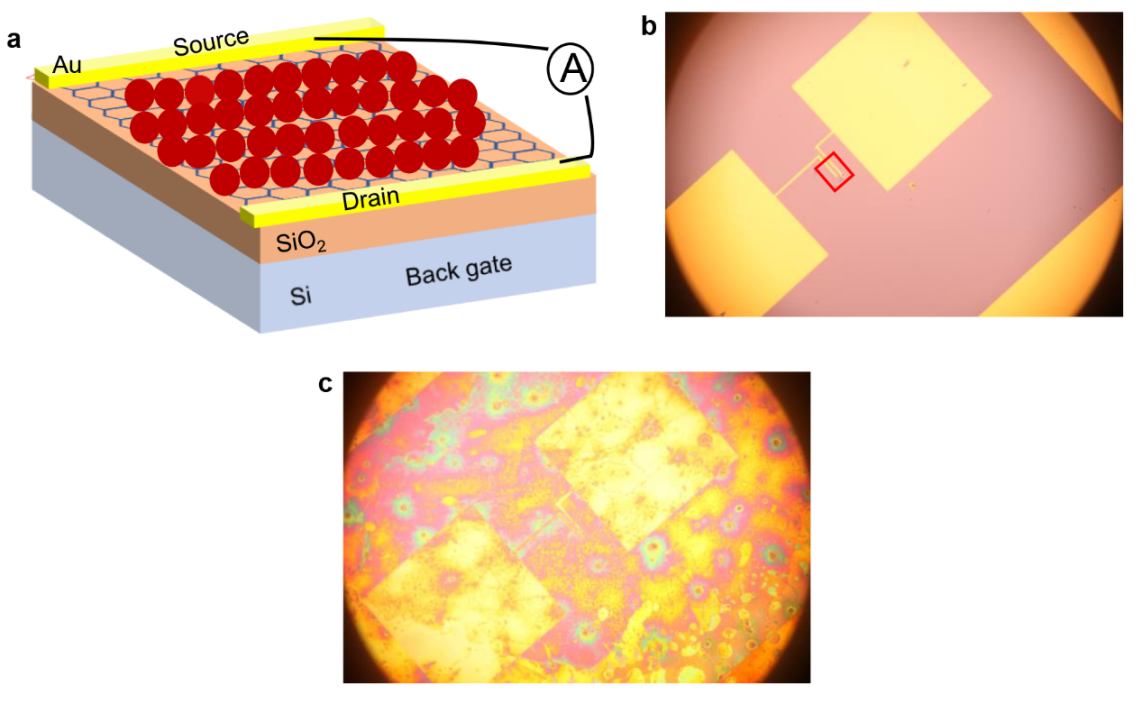
Figure 1: a) Schematic of the proposed device in which a graphene flake is deposited onto a Si/SiO2 structure and coated with PbS quantum dots. b) Optical microscope image of the fabricated graphene FET, and the rectangle with red solid lines inside represents graphene. The effective area of the device is about 10×30 μm2. The golden parts are the source/drain electrodes. c) The optical microscope image of graphene/PbS quantum dots hybrid photodetector.
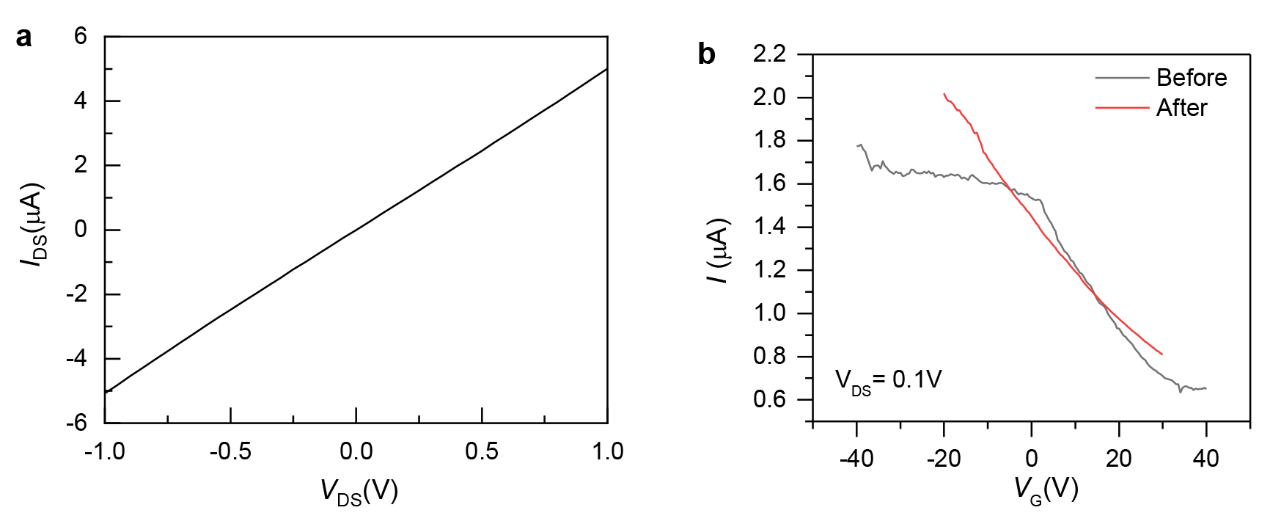
After device fabricated, we tested its electrical properties. Figure 2(a) shows one of the dark current of devices we fabricated, from which we can conclude that there is a good ohmic contact between graphene and electrode. Figure 2(b) shows that changing the back-gate voltage, the current also changes, and the modulation of the Fermi energy level of graphene is achieved. At the same time, spin-coating the quantum dots induces the Dirac peak shift of graphene and changes the graphene mobility. The mobility change of graphene is likely due to increased disorder induced by the quantum dots and the shift of Dirac peak caused by the difference in the work function between graphene and quantum dots.
The photo-detection measurements of our device are illustrated in Figure 3. We first tested pure graphene FET optical response as shown in Figure 3(a). There is no obvious optical response under laser irradiation, because of the low absorption of monolayer graphene. Then we tested the device after PbS quantum dots deposition optical response. It demonstrates that graphene/PbS quantum dots structure is capable of detecting from visible to near-infrared wavelengths. We turn to the specifics of the device and describe the physical mechanism underlying the observed photocurrent response (Figure 3b-d). Quantum dots layer acts as an absorption layer, under the irradiation of light, when the photon energy is above the Fermi energy level energy of the quantum dot, the photon will be absorbed. Photon absorption in PbS quantum dots creates electron– hole pairs, which separate by an internal electric field which induced by the work function mismatch between graphene and the quantum dots. Due to the high charge mobility of graphene and long charge lifetime, the photogenerated electrons or holes will circulate in the graphene channel, leading to photoconductive gain. The photoconductive gain is given by lifetime transit / G τ τ = [19]. From our calculations, we conclude that the responsivity of the device (Rph) can reach to 6.7×10³ A/W, which is calculated by following Rph = Iph/Pin where Iph and Pin represent the photocurrent and incident power, respectively [3].
![Figure 3: We first tested pure graphene FET optical response as shown in Figure 3(a). There is no obvious optical response under laser irradiation, because of the low absorption of monolayer graphene. Then we tested the device after PbS quantum dots deposition optical response. It demonstrates that graphene/PbS quantum dots structure is capable of detecting from visible to near-infrared wavelengths. We turn to the specifics of the device and describe the physical mechanism underlying the observed photocurrent response (Figure 3b-d). Quantum dots layer acts as an absorption layer, under the irradiation of light, when the photon energy is above the Fermi energy level energy of the quantum dot, the photon will be absorbed. Photon absorption in PbS quantum dots creates electron– hole pairs, which separate by an internal electric field which induced by the work function mismatch between graphene and the quantum dots. Due to the high charge mobility of graphene and long charge lifetime, the photogenerated electrons or holes will circulate in the graphene channel, leading to photoconductive gain. The photoconductive gain is given by lifetime transit / G τ τ = [19]. From our calculations, we conclude that the responsivity of the device (Rph) can reach to 6.7×10³ A/W, which is calculated by following Rph = Iph/Pin where Iph and Pin represent the photocurrent and incident power, respectively [3].](/fulltextimages/9889/fig_3.png)
Conclusion
We achieved the detection of visible and near-infrared wavelengths by combining graphene with quantum dots. The process of this approach is simple and low cost. At the same time, the size of quantum dots determines their absorption band, and the modulation of the device band can be achieved by changing the size of quantum dots. Therefore, it is possible to achieve the detection of different wavelengths by this way.
References
-
Ezhilmaran B, Patra A, Benny S, Sreelakshmi MR, Akshay VV, et al. (2021) Recent developments in the photodetector applications of Schottky diodes based on 2D materials. Journal of Materials Chemistry C 9(19): 6122-6150.
-
Guo JX, Lin L, Li SD, Chen JB, Wang SC, et al. (2022) Ferroelectric superdomain controlled graphene plasmon for tunable mid-infrared photodetector with dual-band spectral selectivity. Carbon 189: 596-603.
-
Guo JX, Lin L, Li SD, Chen JB, Wang SC, et al. (2022) WSe2/ MoS2 van der Waals heterostructures decorated with Au nanoparticles for broadband plasmonic photodetectors. Acs Applied Nano Materials 5(1): 587-596.
-
Guo J, Li S, Lin L, Cai J, Chen J, et al. (2022) Enhanced- performance self-powered photodetector based on multi-layer MoS2 sandwiched between two asymmetric graphene contacts. Science China-Technological Sciences 65(11): 2658-2666.
-
Tang X, Ackerman MM, Chen M, Guyot-Sionnest P (2019) Dual-band infrared imaging using stacked colloidal quantum dot photodiodes. Nature Photonics 13(4): 277- 282.
-
Safaei A, Chandra S, Shabbir MW, Leuenberger MN, Chanda D (2019) Dirac plasmon-assisted asymmetric hot carrier generation for room-temperature infrared detection. Nature Communications 10: 3498.
-
Hsu SH (2010) Reflectively Coupled Waveguide Photodetector for High Speed Optical Interconnection. Sensors 10(12): 10863-10875.
-
Eng PC, Song S, Ping B (2015) State-of-the-art photodetectors for optoelectronic integration at telecommunication wavelength. Nanophotonics 4(3): 277-302.
-
Qiu QX, Huang ZM (2021) Photodetectors of 2D Materials from Ultraviolet to Terahertz Waves. Advanced Materials 33(15): 2008126.
-
Dean CR, Young AF, Meric I, Lee C, Wang L, et al. (2010) Boron nitride substrates for high-quality graphene electronics. Nature Nanotechnology 5(10): 722-726.
-
Nair RR, Blake P, Grigorenko AN, Novoselov KS, Booth TJ, et al. (2008) Fine structure constant defines visual transparency of graphene. Science 320(5881): 1308- 1308.
-
Furchi M, Urich A, Pospischil A, Lilley G, Unterrainer K, et al. (2012) Microcavity-Integrated Graphene Photodetector. Nano Letters 12(6): 2773-2777.
-
Guo J, Li J, Liu C, Yin Y, Wang W, et al. (2020) High- performance silicon−graphene hybrid plasmonic waveguide photodetectors beyond 1.55 μm. Light: Science & Applications 9(1): 29.
-
Li LF, Wang JZ, Kang L, Liu W, Yu L, et al. (2020) Monolithic Full-Stokes Near-Infrared Polarimetry with Chiral Plasmonic Metasurface Integrated Graphene- Silicon Photodetector. ACS Nano 14(12): 16634-16642.
-
Li LF, Liu W, Gao AY, Zhao YL, Lu Q, et al. (2019) Plasmon Excited Ultrahot Carriers and Negative Differential Photoresponse in a Vertical Graphene van der Waals Heterostructure. Nano Letters 19(5): 3295-3304.
-
De Fazio D, Uzlu B, Torre I, Monasterio-Balcells C, Gupta S, et al. (2020) Graphene-Quantum Dot Hybrid Photodetectors with Low Dark-Current Readout. ACS Nano 14(9): 11897-11905.
-
Das A, Pisana S, Chakraborty B, Piscanec S, Saha SK, et al. (2008) Monitoring dopants by Raman scattering in an electrochemically top-gated graphene transistor. Nature Nanotechnology 3(4): 210-215.
-
Konstantatos G, Badioli M, Gaudreau L, Osmond J, Bernechea M, et al. (2012) Hybrid graphene-quantum dot phototransistors with ultrahigh gain. Nat Nanotechnol 7(6): 363-368.
-
Grotevent MJ, Hail CU, Yakunin S, Bachmann D, Calame M, et al. (2021) Colloidal HgTe Quantum Dot/Graphene Phototransistor with a Spectral Sensitivity Beyond 3µm. Advanced Science 8(6): 2003360.
- Sense, Gravity, Parity & Chirality in Mathematical Physics
- Quantum Lattice Simulations PHYSICS: Microcircuit Particle Formation and Observable Macroscopic Irreversible Time - A Discrete Lagrangian with Cellular Automata Framework
- Quantum Biology from Biomacromolecule to Cell, and Central Dogma Described by Quantum Theory
- Focus, Agility, Speed and Technology (FAST) for Sustainability and Growth
- Square Root Metric Geometry and Pati-Salam Model in Curved Space-Time
- A Simple System Demonstrating the Mpemba Effect in Classical Mechanics