Comparative Study of the Variation of the Influence of Temperature on Carrier Concentration and Electron Drift on Silicon and Gallium Arsenide
In this paper we have used the theoretical concept to study comparatively the influence of temperature on the electron drift mobility and carrier concentration in silicon and gallium arsenide semiconductor material. From the study as shown in graphs from the computation, it was clearly shown that electron drift current density and carrier concentration vary with temperature. It was also observed that the electron drift current density and carrier concentration decreases and sometimes increases for both materials within some values of temperature which might be attributed to the continual lost of energy by the electron drift velocity resulting from the collision of electrons with ionized impurity atoms and with thermally vibrating atoms.
Introduction
The study of temperature effect on material has revealed that temperature has effect on the conductivity of virtually all materials in all their states because it moderates the electronic motion and lattice vibration of crystal structure that play dominant rule in electrical conduction in any material. However, the real picture of conduction mechanism some of the material especially metals, semiconductor material, is different from the picture as presented in the classical concept [1]. In a semiconductor both mobility and carrier concentration are temperature dependent [2]. This is the reason why it is a common norm that temperature alters the Fermi level of both n-type and p-type of pure and novel Investigation Paper semiconductor material [3] and thereby influencing the overall functionality of the materials. [Ashcroft and 4,1] coupled with the fact that semiconductor is characterized by the activation current carriers either intrinsically or from impurity or both which is an exponential function of temperature. As a result of this, lattice scattering becomes prominent which reduces the mobility of the charge carriers in semiconductor as the temperature increases thereby having explicitly overall effect on the functionality of semiconductor material in all forms [5]. The wide application of Gallium Arsenide and Silicon semiconducting materials in the numerous technological applications such as in the development of nanoparticles [6, 7] and micromaterial had led to veracious study of the various properties of these materials. And again based on the fact that the materials could also be manipulated to suit so many applications some researchers are now engaged in such manipulation [8]. For instance such modification of the surface of semiconductors by laser pulses which has aroused special interest in bio - information technologies [9] that has led invariably for the special interest in the study of the properties of these semiconductor materials coupled with the fact that some of the equipment made from these materials are operated at different temperature in different places around the of Globe has led us to theoretically examine the influence of temperature on electrical conductivity of these materials in question.
In course of this study we consider the distribution of electrons in the conduction band is given by the density of allowed quantum states times the probability that a state will be occupied $$ n (E) = g _ {c} (E) F (E) \tag {1} $$ The thermal equilibrium concentration of electrons number is given by $$ n _ {0} = \int_ {0} ^ {\infty} z $$ ()() E F E g n c ∫ (2) c E The density of state in the conduction band is given by
2 1 $$ V = \frac {4 \pi}{h ^ {3}} \left(2 m _ {e} ^ {*}\right) ^ {\frac {3}{2}}. $$ () ( ) dE E m h dE E g e c The bottom edge of the conduction band correspond to the potential energy of an electron at rest thus C E E − will be the kinetic energy of the conduction band at the higher energy level.
$$ g _ {c} (E) d E = \frac {4 \pi}{h ^ {3}} \left(2 m _ {e} ^ {*}\right) ^ {\frac {3}{2}} E - E _ {c} ^ {\frac {1}{2}} d E $$
| 2 | EE c |
|---|
For electrons in conduction band, if , KT E E f c −
then KT E E f − for Fermi energy within the band gap. Hence the Fermi probability function reduces to the Boltzmann approximation Ugwu EI. Comparative Study of the Variation of the Influence of Temperature on Carrier Concentration and Electron Drift on Silicon and Gallium Arsenide. Nanomed Nanotechnol 2019, 4(2): 000162.
() ( ) [ ] f − − exp
E E E F KT (4)
Subsisting for value of () E gc and () E F in equation (2)
( ) ( )dE KT ∞ exp 2 4 2 3
$$ = \int_ {E _ {C}} ^ {\infty} \frac {4 \pi \left(2 m _ {e} ^ {*}\right) ^ {\frac {3}{2}}}{h ^ {3}} \sqrt {E - E _ {c}} \exp \left[ \frac {- \left(E - I\right)}{K T} \right] $$ E E E E h * π m n f c E e o C
3 ( )
$$ = 2 \left(\frac {2 \pi m _ {e} ^ {*} K T}{h ^ {2}}\right) \exp \left[ \frac {- \left(E _ {C} - 1\right)}{K T} \right] $$ − − π * E E h KT m n F C e exp 2 2 2
( ) $$ \Rightarrow n _ {0} = N _ {c} \exp \left[ \frac {- \left(E _ {c} - I\right)}{K T} \right] $$ E E N n f c c exp
0 KT (5) Similarly, the distribution of holes in the valence band is given by the density of allowed quantum state times the probability that a state will not be occupied by an electron $$ P (E) = g _ {v} (E) \left[ 1 - F (E) \right] \tag {6} $$ And the thermal equilibrium concentration of holes o p is given by (7) () () [ ] E F E g P v E $$ P _ {0} = \int_ {- \infty} ^ {E _ {v}} g _ {v} (E) [ 1 - I $$ The density of state in the valence band is given by
2 1 $$ \because = \frac {4 \pi}{h ^ {3}} \left(2 m _ {p} ^ {*}\right) $$
() ( ) dE E m h dE E g p v
2 3 Hence,
| 2 | EE V |
|---|
The top edge of the valence band V E correspond to the potential energy of a hole at rest, thus E EV − will be the kinetic energy of the hole at lower energy level For energy state in the valence band, 0 E E . If ( ) KT E E v f − () ( ) − − ≈ − KT E E E F f exp 1 (9) Copyright© Ugwu EI.
Substituting for the value of () E gc and 1- () E F in equation (7)
| p 3 | E E v |
|---|
dE KT
0 ∞ − Then
( )
2 3 − −
=
E E π KT M P
exp 2 2 v f p
2 0 KT h
2 3 =
2 π KT M N
2 2 p v
`where h ( )
$$ \Rightarrow P _ {0} = N _ {v} \exp \left[ \frac {- \left(E _ {f} - I\right)}{K T} \right] $$ E E N P v f v exp
0 KT (10) For intrinsic semiconductor, = =
$$ \begin{array}{l} n = p = n _ {i} \\ n _ {0} = p _ {0} \\ \end{array} $$
0 0 p n Number of 1 − e in Conduction band = number of holes in valence band due to the fact that when 1 − e makes a transition to the CB it leaves a hole behind in the VB.
$$ \mathrm {H e n c e}, n _ {0} * p _ {0} = n _ {I} ^ {2} $$
Where ( )
$$ \begin{array}{l} n _ {0} = N _ {c} \exp \left[ \frac {- \left(E _ {c} - E _ {f}\right)}{K T} \right] \\ p _ {0} = N _ {v} \exp \left[ \frac {- \left(E _ {c} - E _ {v}\right)}{K T} \right] \\ \Rightarrow n _ {i} ^ {2} = N _ {c} \exp \left[ \frac {- \left(E _ {c} - E _ {f}\right)}{K T} \right] N _ {v} \exp \left[ \frac {- \left(E _ {f} - E _ {v}\right)}{K T} \right] \\ n _ {i} ^ {2} = \sqrt {N _ {C} N _ {v}} \exp \left[ \frac {- \left(E _ {c} - E _ {v}\right)}{2 K T} \right] \\ \end{array} $$ E E n N KT c f c exp
0 ( ) E E p N KT
c v v exp
0 ( ) ( ) E E E E n N N KT KT
c f f v i c v
2 exp exp ( ) E E n N N KT
c v i C v
2 exp 2 − = E E E
v c g − =
E N N n Where
g v c i
2 exp KT − = KT
E N N n
g V C i 2 exp 2 1
( ) (11) Substituting for C N and V N in equation (11)
Ugwu EI. Comparative Study of the Variation of the Influence of Temperature on Carrier Concentration and Electron Drift on Silicon and Gallium Arsenide. Nanomed Nanotechnol 2019, 4(2): 000162.
1 3 3 2 2 2
$$ = \left[ 2 \left(\frac {2 \pi m _ {n} ^ {*} K T}{h ^ {2}}\right) ^ {\frac {3}{2}} \cdot 2 \left(\frac {2 \pi m _ {p} ^ {*} K T}{h ^ {2}}\right) ^ {\frac {3}{2}} \right] ^ {\frac {1}{2}} \exp \left[ \frac {- E _ {g}}{2 K T} \right] $$ π π
2 2 2 2 2 2 exp 2
m KT E m KT n h h KT
p g n i
2 1
2 3
− π π
E KT m g p n i 2 exp 2 2 4
KT m n
• =
2 2 KT h h
2 1
2 3 2 3 −
$$ = \left| 4 \left(\frac {4 \pi^ {2} k ^ {2} T ^ {2}}{b ^ {4}}\right) ^ {\frac {5}{2}} \left(m _ {n} ^ {*} m _ {p} ^ {*}\right) \right| $$ E m m h
2 2 2 π ( )
T k n g p n i 2 exp 4 4
4 KT g p n i 2 exp 2 2 4 3 2 3
$$ = 2 \left(\frac {2 \pi K T}{h ^ {2}}\right) ^ {\frac {3}{2}} \left(m _ {n} ^ {*} m _ {p} ^ {*}\right) ^ {\frac {3}{4}} \exp \left[ \frac {- I}{2 K} \right] $$ E m m h
2 π ( )
KT n KT (12) Equation12 is the expression explaining the distribution of carrier concentration is given in equation.
While that of total drift current density relating to both electrons as a major carries and hole as minority carries can be expressed as $$ J _ {\mathrm {d r f}} = \mathrm {e} \left(\mu_ {\mathrm {n}} \mathrm {n} + \mu_ {\mathrm {p}} \mathrm {p}\right) \mathrm {E} \tag {13} $$ The drift current density due to electron is given as $$ J _ {\mathrm {n} / \mathrm {d r f}} = \mathrm {e} \mu_ {\mathrm {n}} \mathrm {n E} \tag {14} $$ Where n is known as the electron density of the conduction band and is given as $$ n = N _ {\mathrm {C}} \exp \frac {- \left(E _ {\mathrm {c}} - E _ {\mathrm {f}}\right)}{\mathrm {K T}} \tag {15} $$ c f C Combing equations (14) and 15) we obtain $$ J _ {\mathrm {n} / \mathrm {d r f}} = \mathrm {e} \mu_ {\mathrm {n}} \mathrm {E N} _ {\mathrm {c}} \exp \frac {- \left(\mathrm {E} _ {\mathrm {c}} - \mathrm {E} _ {\mathrm {f}}\right)}{\mathrm {K T}} \tag {16} $$ c f n/drf n c
Result
The expression explaining the distribution of carrier concentration is given in equation (12) while that of electron drift mobility is that of equation (16) and the result of the computation for 300k to 800k were showcased in Tables 1-12 while the graphs were plotted for both Gallium Arsenide and Silicon particular band gap and respectively.
Copyright© Ugwu EI.
- 2∏
- KB
- T h2 mn* mp*
- Eg ni
- 6.284
- 1.38×10⁻²³
- 300
- 4.3904×10-67
- 1.182
- 0.81
- 0.91
- 7.91×10¹⁷
- 6.284
- 1.38×10⁻²³
- 400
- 4.3904×10-67
- 1.182
- 0.81
- 0.91
- 9.88×10¹⁹
- 6.284
- 1.38×10⁻²³
- 500
- 4.3904×10-67
- 1.182
- 0.81
- 0.91
- 1.93×10²¹
- 6.284
- 1.38×10⁻²³
- 600
- 4.3904×10-67
- 1.182
- 0.81
- 0.91
- 1.47×10²²
- 6.284
- 1.38×10⁻²³
- 700
- 4.3904×10-67
- 1.182
- 0.81
- 0.91
- 6.52×10²²
- 6.284
- 1.38×10⁻²³
- 800
- 4.3904×10-67
- 1.182
Table 4: Intrinsic carrier concentration for silicon for
- Eg
- 91
- .0
-
- 2∏
- KB
- T h2 mn* mp*
- Eg ni
- 6.284
- 1.38×10⁻²³
- 300
- 4.3904×10-67
- 1.182
- 0.81
- 1.11
- 1.66×10⁻¹⁶
- 6.284
- 1.38×10⁻²³
- 400
- 4.3904×10-67
- 1.182
- 0.81
- 1.11
- 5.44×10¹⁸
- 6.284
- 1.38×10⁻²³
- 500
- 4.3904×10-67
- 1.182
- 0.81
- 1.11
- 1.9×10²⁰
- 6.284
- 1.38×10⁻²³
- 600
- 4.3904×10-67
- 1.182
- 0.81
- 1.11
- 2.13×10²¹
- 6.284
- 1.38×10⁻²³
- 700
- 4.3904×10-67
- 1.182
- 0.81
- 1.11
- 1.24×10²²
- 6.284
- 1.38×10⁻²³
- 800
- 4.3904×10-67
- 1.182
- 0.81
- 1.11
- 4.79×10²²
Table 5: Intrinsic carrier concentration for silicon for
- Eg
- 11
- .1
-
- 2∏
- KB
- T h2 mn* mp*
- Eg ni
- 6.284
- 1.38×10⁻²³
- 300
- 4.3904×10-67
- 1.182
- 0.81
- 1.33
- 2.36×10¹⁴
- 6.284
- 1.38×10⁻²³
- 400
- 4.3904×10-67
- 1.182
- 0.81
- 1.33
- 2.25×10¹⁴
- 6.284
- 1.38×10⁻²³
- 500
- 4.3904×10-67
- 1.182
- 0.81
- 1.33
- 1.48×10¹⁹
- 6.284
- 1.38×10⁻²³
- 600
- 4.3904×10-67
- 1.182
- 0.81
- 1.33
- 2.55×10²⁰
- 6.284
- 1.38×10⁻²³
- 700
- 4.3904×10-67
- 1.182
- 0.81
- 1.33
- 2.01×10²¹
- 6.284
- 1.38×10⁻²³
- 800
- 4.3904×10-67
- 1.182
- 0.81
- 1.33
- 9.74×10²¹
Table 6: Intrinsic carrier concentration for silicon for
- Eg
- 33
- .1
-
- 2∏
- KB
- T h2 mn* mp*
- Eg ni
- 6.284
- 1.38×10⁻²³
- 300
- 4.3904×10-67
- 0.065
- 0.524
- 1.2
- 2.39×10¹⁴
- 6.284
- 1.38×10⁻²³
- 400
- 4.3904×10-67
- 0.065
- 0.524
- 1.2
- 1.2×10¹⁷
- 6.284
- 1.38×10⁻²³
- 500
- 4.3904×10-67
- 0.065
- 0.524
- 1.2
- 5.48×10¹⁸
- 6.284
- 1.38×10⁻²³
- 600
- 4.3904×10-67
- 0.065
- 0.524
- 1.2
- 7.32×10¹⁹
- 6.284
- 1.38×10⁻²³
- 700
- 4.3904×10-67
- 0.065
- 0.524
- 1.2
- 4.83×10²⁰
- 6.284
- 1.38×10⁻²³
- 800
- 4.3904×10-67
- 0.065
- 0.524
- 1.2
- 2.05×10²¹
Table 7: Intrinsic carrier concentration for gallium arsenide for
- Eg
- 2.1
-
- 2∏
- KB
- T h2 mn* mp*
- Eg ni
- 6.284
- 1.38×10⁻²³
- 300
- 4.3904×10-67
- 0.065
- 0.524
- 1.43
- 2.8×10¹²
- 6.284
- 1.38×10⁻²³
- 400
- 4.3904×10-67
- 0.065
- 0.524
- 1.43
- 4.32×10¹⁵
- 6.284
- 1.38×10⁻²³
- 500
- 4.3904×10-67
- 0.065
- 0.524
- 1.43
- 3.81×10¹⁷
- 6.284
- 1.38×10⁻²³
- 600
- 4.3904×10-67
- 0.065
- 0.524
- 1.43
- 7.93×10¹⁸
- 6.284
- 1.38×10⁻²³
- 700
- 4.3904×10-67
- 0.065
- 0.524
- 1.43
- 7.2×10¹⁹
- 6.284
- 1.38×10⁻²³
- 800
- 4.3904×10-67
- 0.065
- 0.524
- 1.43
- 3.86×10²⁰
- 2∏
- KB
- T h2 mn* mp*
- Eg ni
- 6.284
- 1.38×10⁻²³
- 300
- 4.3904×10-67
- 0.065
- 0.524
- 1.6
- 1.05×10¹¹
- 6.284
- 1.38×10⁻²³
- 400
- 4.3904×10-67
- 0.065
- 0.524
- 1.6
- 3.67×10¹⁴
- 6.284
- 1.38×10⁻²³
- 500
- 4.3904×10-67
- 0.065
- 0.524
- 1.6
- 5.31×10¹⁶
- 6.284
- 1.38×10⁻²³
- 600
- 4.3904×10-67
- 0.065
- 0.524
- 1.6
- 1.54×10¹⁸
- 6.284
- 1.38×10⁻²³
- 700
- 4.3904×10-67
- 0.065
- 0.524
- 1.6
- 1.76×10¹⁹
- 6.284
- 1.38×10⁻²³
- 800
- 4.3904×10-67
- 0.065
- 0.524
- 1.6
- 1.13×10²⁰
Table 8: Intrinsic carrier concentration for gallium arsenide for
Ugwu EI. Comparative Study of the Variation of the Influence of Temperature on Carrier Concentration and Electron Drift on Silicon and Gallium Arsenide. Nanomed Nanotechnol 2019, 4(2): 000162.
Copyright© Ugwu EI.
- Eg
- 6.1
-
- Temperature (K) e( c )
- E(v/cm) µn(cm2/V-S)
- Nc(cm-3)
- (Ec-Ef)
- Jn/drf(amp/cm2)
- 300
- 1.602×10⁻¹⁹
- 5
- 1350
- 2.8162×10¹⁹
- 4.2865×10⁻²¹
- 10813.521
- 400
- 1.602×10⁻¹⁹
- 5
- 1350
- 4.3357×10¹⁹
- 8.0972×10⁻²¹
- 10813.489
- 500
- 1.602×10⁻¹⁹
- 5
- 1350
- 6.0594×10¹⁹
- 1.2431×10⁻²⁰
- 10813.523
- 600
- 1.602×10⁻¹⁹
- 5
- 1350
- 7.9653×10¹⁹
- 1.7182×10⁻²⁰
- 10813.217
- 700
- 1.602×10⁻¹⁹
- 5
- 1350
- 1.0037×10²⁰
- 2.2279×10⁻²⁰
- 10813.106
- 800
- 1.602×10⁻¹⁹
- 5
- 1350
- 1.2263×10²⁰
- 2.7673×10⁻²⁰
- 10813.222
-
Table 9: Electron drift mobility for Si at
-
-
-
-
- 18
- 3 d
- N
- 10 cm
- N
- 4 10 cm
- 13
- 3 d
- Temperature (K) e( c )
- E(v/cm) µn(cm2/V-S)
- Nc(cm-3)
- (Ec-Ef)
- Jn/drf(amp/cm2)
- 300
- 1.602×10⁻¹⁹
- 5
- 8500
- 4.3514×10¹⁷
- -1.2978×10⁻²⁰
- 68092.494
- 400
- 1.602×10⁻¹⁹
- 5
- 8500
- 6.6995×10¹⁷
- -1.4921×10⁻²⁰
- 68081.080
- 500
- 1.602×10⁻¹⁹
- 5
- 8500
- 9.3628×10¹⁷
- -1.6342×10⁻²⁰
- 68083.638
- 600
- 1.602×10⁻¹⁹
- 5
- 8500
- 1.2308×10¹⁸
- -1.7346×10⁻²⁰
- 68085.464
- 700
- 1.602×10⁻¹⁹
- 5
- 8500
- 1.5509×10¹⁸
- -1.8004×10⁻²⁰
- 68086.255
- 800
- 1.602×10⁻¹⁹
- 5
- 8500
- 1.8949×10¹⁸
- -1.8364×10⁻²⁰
- 68084.099
Table 10: Electron drift mobility for GaAs at
- 19
- 3 d
- N
- 10 cm
-
- Temperature (K) e( c )
- E(v/cm) µn(cm2/V-S)
- Nc(cm-3)
- (Ec-Ef)
- Jn/drf(amp/cm2)
- 300
- 1.602×10⁻¹⁹
- 5
- 1350
- 2.8162×10¹⁹
- 1.3819×10⁻²⁰
- 10813.405
- 400
- 1.602×10⁻¹⁹
- 5
- 1350
- 4.3357×10¹⁹
- 2.0807×10⁻²⁰
- 10813.441
- 500
- 1.602×10⁻¹⁹
- 5
- 1350
- 6.0594×10¹⁹
- 2.8319×10⁻²⁰
- 10813.542
- 600
- 1.602×10⁻¹⁹
- 5
- 1350
- 7.9653×10¹⁹
- 3.6247×10⁻²⁰
- 10813.375
- 700
- 1.602×10⁻¹⁹
- 5
- 1350
- 1.0037×10²⁰
- 4.4522×10⁻²⁰
- 10813.307
- 800
- 1.602×10⁻¹⁹
- 5
- 1350
- 1.2263×10²⁰
- 5.3093×10⁻²⁰
- 10813.375
Table 11: Electron drift mobility for Si at
Temperature (K) e( c ) E(v/cm) µn(cm2/V-S) Nc(cm-3) (Ec-Ef) Jn/drf(amp/cm2) 300 1.602×10⁻¹⁹ 5 8500 4.3514×10¹⁷ -3.4448×10⁻²¹ 6808.431 400 1.602×10⁻¹⁹ 5 8500 6.6995×10¹⁷ -2.2110×10⁻²¹ 6808.441 500 1.602×10⁻¹⁹ 5 8500 9.3628×10¹⁷ -4.5430×10⁻²² 6808.499 600 1.602×10⁻¹⁹ 5 8500 1.2308×10¹⁸ 1.7195×10⁻²¹ 6808.468 700 1.602×10⁻¹⁹ 5 8500 1.5509×10¹⁸ 4.2392×10⁻²¹ 6808.465 800 1.602×10⁻¹⁹ 5 8500 1.8949×10¹⁸ 7.0564×10⁻²¹ 6808.496 Ugwu EI. Comparative Study of the Variation of the Influence of Temperature on Carrier Concentration and Electron Drift on Silicon and Gallium Arsenide. Nanomed Nanotechnol 2019, 4(2): 000162.
Copyright© Ugwu EI.
- 17
- 3 d
- N
- 1.34 10 cm
-
-
- Temperature (K) e( c )
- E(v/cm) µn(cm2/V-S)
- Nc(cm-3)
- (Ec-Ef)
- Jn/drf(amp/cm2)
- 300
- 1.602×10⁻¹⁹
- 5
- 1350
- 2.8162×10¹⁹
- 2.2140×10⁻²⁰
- 144.910
- 400
- 1.602×10⁻¹⁹
- 5
- 1350
- 4.3357×10¹⁹
- 3.1902×10⁻²⁰
- 144.906
- 500
- 1.602×10⁻¹⁹
- 5
- 1350
- 6.0594×10¹⁹
- 4.2187×10⁻²⁰
- 144.909
- 600
- 1.602×10⁻¹⁹
- 5
- 1350
- 7.9653×10¹⁹
- 5.2889×10⁻²⁰
- 144.906
- 700
- 1.602×10⁻¹⁹
- 5
- 1350
- 1.0037×10²⁰
- 6.3937×10⁻²⁰
- 144.907
- 800
- 1.602×10⁻¹⁹
- 5
- 1350
- 1.2263×10²⁰
- 7.5283×10⁻²⁰
- 144.897
Table 12: Electron drifts mobility for Si at
- 18
- 3 d
- N
- 10 cm
-
- Temperature (K) e( c )
- E(v/cm) µn(cm2/V-S)
- Nc(cm-3)
- (Ec-Ef)
- Jn/drf(amp/cm2)
- 300
- 1.602×10⁻¹⁹
- 5
- 8500
- 4.3514×10¹⁷
- 4.8764×10⁻²¹
- 912.34
- 400
- 1.602×10⁻¹⁹
- 5
- 8500
- 6.6995×10¹⁷
- 8.8837×10⁻²¹
- 912.337
- 500
- 1.602×10⁻¹⁹
- 5
- 8500
- 9.3628×10¹⁷
- 1.3414×10⁻²⁰
- 912.354
- 600
- 1.602×10⁻¹⁹
- 5
- 8500
- 1.2308×10¹⁸
- 1.8362×10⁻²⁰
- 912.291
- 700
- 1.602×10⁻¹⁹
- 5
- 8500
- 1.5509×10¹⁸
- 2.3655×10⁻²⁰
- 912.333
- 800
- 1.602×10⁻¹⁹
- 5
- 8500
- 1.8949×10¹⁸
- 2.9264×10⁻²⁰
- 912.327
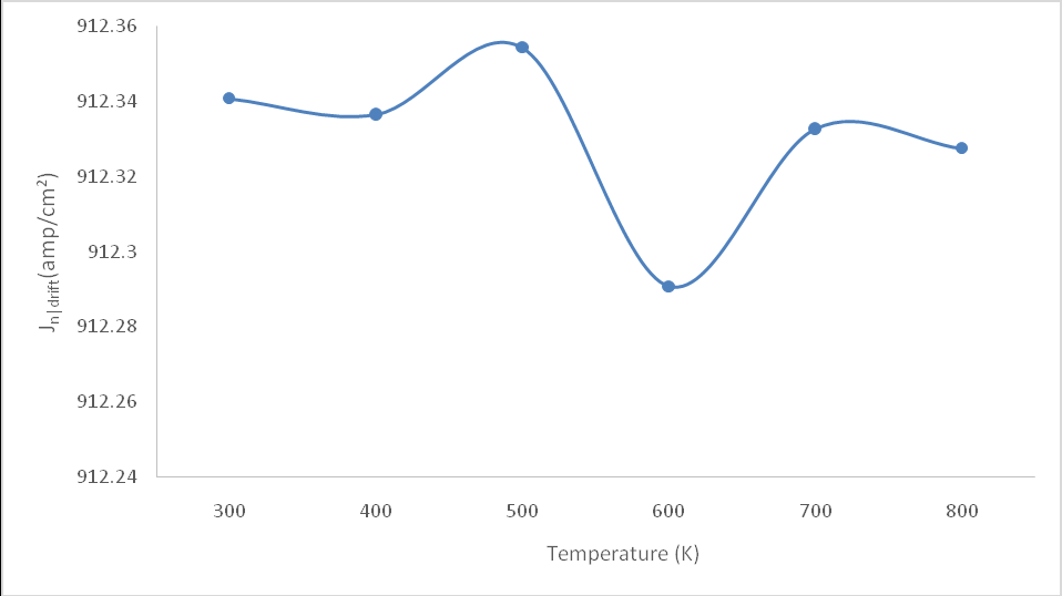
Table 13: Electron drift mobility for Silicon at
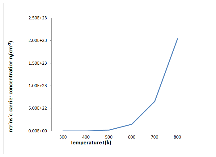
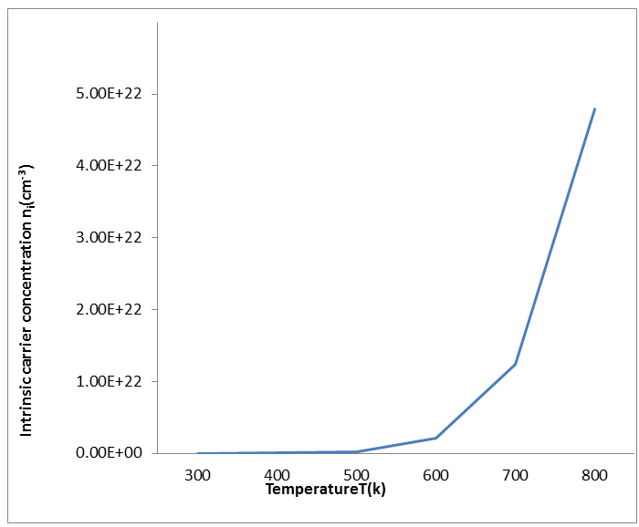
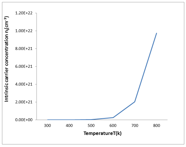
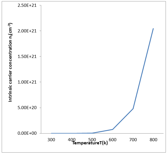
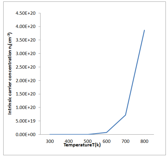
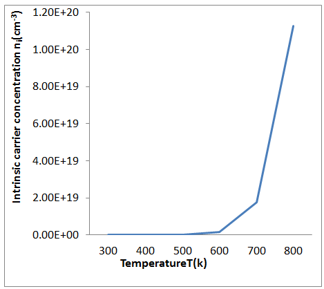
Figures 1, 2 and 3, indicate the intrinsic carrier concentrations are plotted against temperature for silicon for a given energy band gap which was computed from equation 12. At temperature below 300k, electrons do not receive enough energy to break a bond and remain in the valence band. Thus in all these figures, it is observed that electrons remains in the valence band due to lack of enough thermal energy. The electron concentration in the conduction band is very low, but as the temperature is increased the number bonds (carriers) increases because there is more thermal energy available so more electron gain energy to break through the energy band gap and get from valence band to conduction band in the same way as in silicon, it is observed that at higher temperature about 400k and 500K, electron-hole pair generation becomes so high that intrinsic concentration becomes comparable to donor concentration such that intrinsic contribution becomes non-negligible and rapidly dominates. In a similar manner, Figures 4-6 shows the graphs of intrinsic carrier concentration against temperature for gallium arsenide for a given energy band gap. Just like Silicon, at temperature 300k, electrons do not receive enough energy to tunnel through the energy band gap to the Ugwu EI. Comparative Study of the Variation of the Influence of Temperature on Carrier Concentration and Electron Drift on Silicon and Gallium Arsenide. Nanomed Nanotechnol 2019, 4(2): 000162.
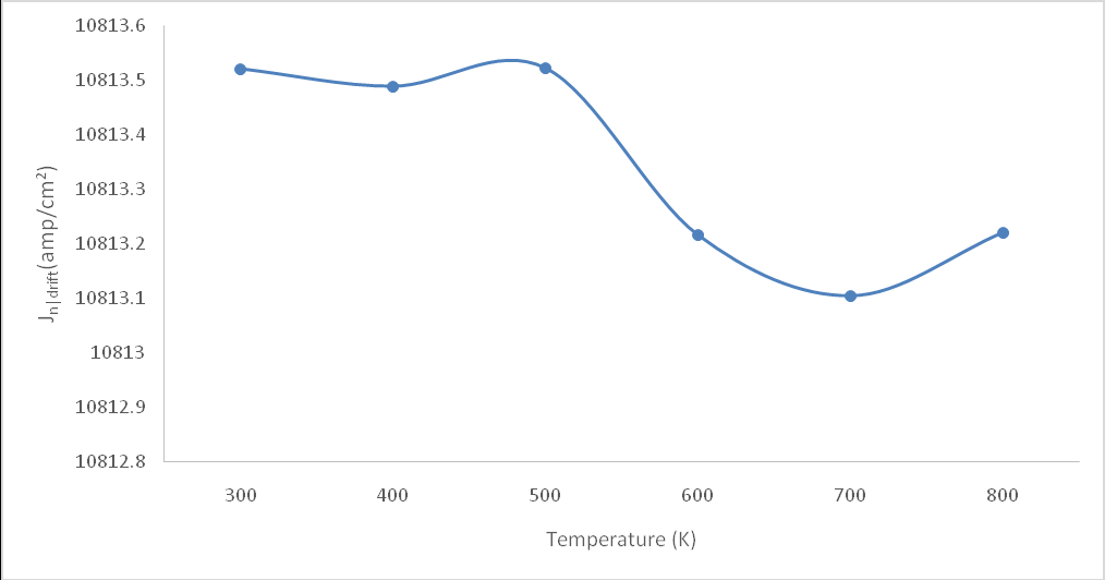
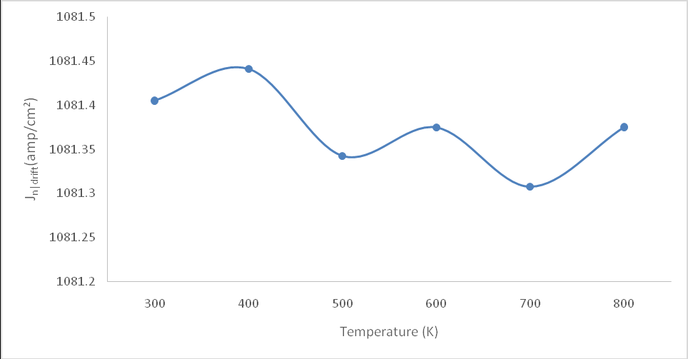
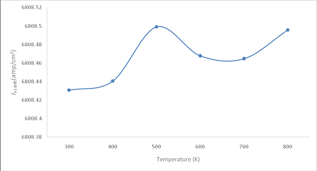
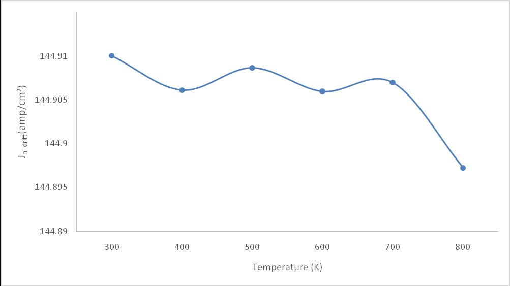
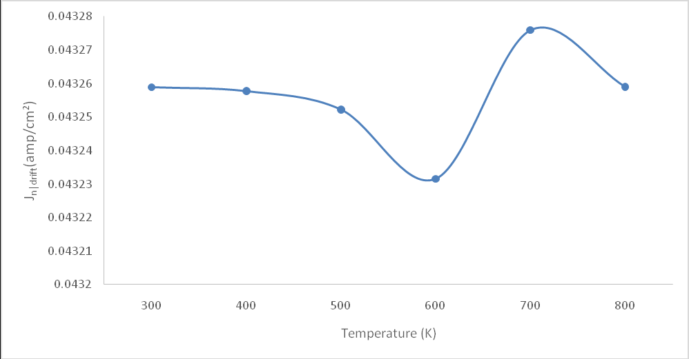
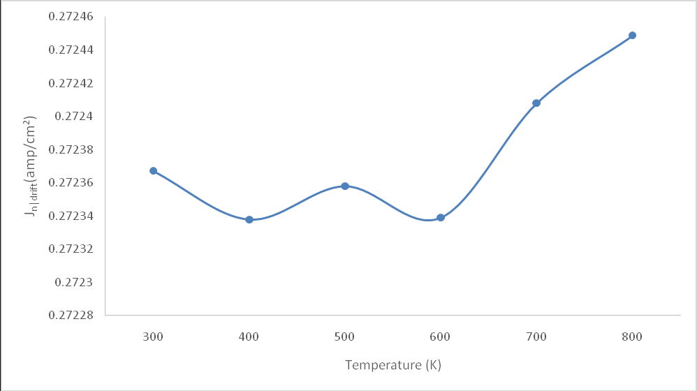
The computation of electron drift mobility as function of temperature was obtained from equation 16 for both silicon and gallium arsenide considering the temperature ranges of 300k to 800k for given Nd . While the graphs as showcased in Figure 7-14 did not follow a particular trend as it was seen that the variation of the electron drift with temperature for different carrier concentration, Nd for both GaAs and Si did not trail a definite pattern but rather alternated irregularly. Sometimes, the electron drift was found to be higher at high temperature range, 450k to 800k for some values of Nd while in some cases it was found to be higher at lower temperature range, between 300k to 500k.
Copyright© Ugwu EI.
$$ E _ {g} = 1. 1 1 e v $$
$$ E _ {g} = 1. 3 3 e v $$ Ugwu EI. Comparative Study of the Variation of the Influence of Temperature on Carrier Concentration and Electron Drift on Silicon and Gallium Arsenide. Nanomed Nanotechnol 2019, 4(2): 000162.
Copyright© Ugwu EI.
Ugwu EI. Comparative Study of the Variation of the Influence of Temperature on Carrier Concentration and Electron Drift on Silicon and Gallium Arsenide. Nanomed Nanotechnol 2019, 4(2): 000162.
$$ E _ {g} = 1. 6 e v $$
drf n J | Figure 7: The Graph of
as a Function of Temperature for Si at
$$ \mathrm {N} _ {\mathrm {d}} = 1 0 ^ {1 9} \mathrm {c m} ^ {- 3} $$
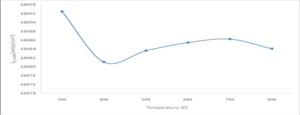
drf n J | Figure 8: The Graph of
as a Function of Temperature for GaAs at
$$ \mathrm {N} _ {\mathrm {d}} = 1 0 ^ {1 9} \mathrm {c m} ^ {- 3} $$
drf n J | Figure 9: The Graph of as a Function of Temperature for Si at 18 3 d N 10 cm− = Ugwu EI. Comparative Study of the Variation of the Influence of Temperature on Carrier Concentration and Electron Drift on Silicon and Gallium Arsenide. Nanomed Nanotechnol 2019, 4(2): 000162.
Copyright© Ugwu EI.
drf n J | Figure 10: The Graph of
as a function of Temperature for GaAs at
$$ N _ {\mathrm {d}} = 1 0 ^ {1 8} \mathrm {c m} ^ {- 3} $$
Copyright© Ugwu EI.
drf n J | $$ \mathrm {N} _ {\mathrm {d}} = 4 \times 1 0 ^ {1 3} \mathrm {c m} ^ {- 3} $$ Figure 13: The Graph of as a Function of Temperature for Si at
Ugwu EI. Comparative Study of the Variation of the Influence of Temperature on Carrier Concentration and Electron Drift on Silicon and Gallium Arsenide. Nanomed Nanotechnol 2019, 4(2): 000162.
Summary
From the report as enshrined in the graphs of the work indicated that at a given temperature below 300k, the electron ca not move from valence band to conduction band for a particular band gap which is an indication that there is a threshold temperature at which carrier concentration in these material is affected. However in the case of electron drift, it was clearly observed that the variation of electron drift did not define a particular trend as the temperature varies because it was seen that sometimes, electron drift was found to be higher at higher temperature while in some cases it was higher at lower temperature. Therefore comparatively, it has been clearly seen that intrinsic carrier concentration is more temperature dependent at given energy band gap than the electron drift mobility at a given $N_d$.
References
-
Pillia SO (2010) Solid State Physics, New Revised Edition, New age International (p) Ltd Publishers, New Delhi, pp: 521-530.
-
Donald AN (2003) Semiconductor Physics and Devices: Basic Principles 3rd (edn), McGraw-Hill Higher Education.
-
Blakemore JS (1982) Approximations for Fermi-Dirac integrals, especially the function $\frac{\xi}{1/2(\eta)}$, used to describe electron density in a semiconductor, Solid-State Electronics 25(11): 1067-1076.
-
Ashcroft NW, Mermin ND (1976) Solid state physics, Saunders College, Vol 1.
-
Martin AG (1987) Solar Cells: Operating Principles, Technology, and System Applications. Englewood Cliffs: Prentice-Hall Inc.
-
Zywietz U, Evlyukhin AB, Reinhardt C, Chichkov BN (2014) Laser printing of silicon nanoparticles with resonant optical electric and magnetic responses. Nat Communs 5: 3402-3405.
-
Sze SM, Ng Kwok (2007) Physics of Semiconductor Devices, John Wiley & Sons.
-
Wagne J, del Alamo JA (1988) Band-gap narrowing in heavily doped silicon: A comparison of optical and electrical data. J Appl Phys 63(2): 425-429.
-
Bhuyan MK, Courvoisier FP, Lacourt A, Jacquot M, Salut R, et al. (2010) High aspect ratio nanochannel machining using single shot femtosecond Bessel beams. Appl Phys Lett 97(8): 081102.
- Solution-Processed Chiral Perovskites for Biomedical Applications
- Nanotechnology in Health Chemistry and Medicine: Current Challenges and Future Directions
- Human Exposure to Micro- and Nanoplastics: Pathways, Toxicity, and Intervention Strategies
- Exosome Nanomedicine for Cancer Therapy
- Micro and Nanoplastics–Plastisphere, Biotoxicity, Impact on Human Health, and Mitigation Strategies
- Process Validation of Cefixime Powder for Suspension Dosage Form, 50 mL