Choice of Material for Sensor: Nanostructured Zinc Oxide
To study and develop the fundamentals of the gas sensing mechanism, the semiconducting sensors are modified by simple addition of metals (Al, In, Cu, Sn, Fe, Ru, Pt, Pd, etc.), in the base materials, which is referred as doping. Metal oxides such as ZnO, SnO2 , Fe2 O3 , TiO2 , WO3 etc. have also been used as gas sensors. Despite these broad studies in the semiconductor sensor area, problems such as poor gas selectivity, inability to detect the trace amount of gas (ppm/ ppb), and degradation of the sensor performance by surface contamination still persist. Thus, there is growing need for nanocrystalline gas sensors with novel properties.
Editorial
To study and develop the fundamentals of the gas sensing mechanism, the semiconducting sensors are modified by simple addition of metals (Al, In, Cu, Sn, Fe, Ru, Pt, Pd, etc.), in the base materials, which is referred as doping. Metal oxides such as ZnO, SnO2, Fe2O3, TiO2, WO3 etc. have also been used as gas sensors. Despite these broad studies in the semiconductor sensor area, problems such as poor gas selectivity, inability to detect the trace amount of gas (ppm/ ppb), and degradation of the sensor performance by surface contamination still persist. Thus, there is growing need for nanocrystalline gas sensors with novel properties.
One material that has been in great interest from wide range of technological field associated with nanotechnology is zinc oxide (ZnO) [1]. It is an important and versatile functional material having a wide band gap (3.37 eV) with large exciton energy (60 meV) at room temperature. The ZnO wurtzite structure has a hexagonal closed-packed unit cell, with dimensions a = 3.25 Å and c = 5.12 Å [2]. The structure can be visualized as Zn2+ ions in half of the tetrahedral holes of a hexagonal close-packed oxide lattice; the structure with the longitudinal axis (c-axis) is shown in Figure 1.
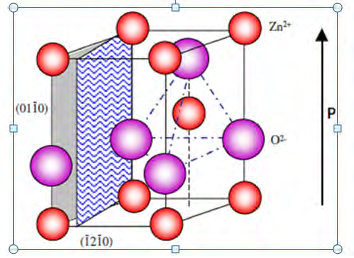
In this crystal structure, both zinc and oxygen ions are coordinated with four ions of the opposite charge with strong ionic binding. Due to the size differential of the ions, the ions fill about 44% of the total volume in a ZnO crystal, and leaving a relatively large free volume.
ZnO is a versatile semiconductor material, which has attracted attention for its wide range of technological applications such as solar cells [3], luminescent, electrical and acoustic devices and chemical sensors [4]. Semiconducting sensors offer an inexpensive and simple method for monitoring gases. To date, various types of ZnO-based gas sensors, such as thick films [5], thin films [6], nanoparticles [7], nanorods [8] and heterojunctions [9], have been demonstrated. Some dangerous and poisonous gases, e.g., hydrogen, LPG, carbon monoxide and methane, etc., could be detected [10]. A wide number of methods have been used to prepare ZnO powders, including, homogeneous precipitation in aqueous solution of Zn2+ cations, solution combustion [11], freeze- drying [12], dc magnetron sputtering [13], chemical growth [14] and sol-gel [15]. ZnO thin films were prepared by various techniques such as sol-gel [16], sputtering [17], laser ablation [18], chemical bath deposition [19] and spray pyrolysis [20].
ZnO is a typical n-type semiconductor, in which the density of holes in the valence band is exceeded by the density of electrons in the conduction band; the major charge carrier in ZnO semiconductors is electrons in the conduction band. The formation of oxygen vacancies leads to a higher electron density; donor bands from vacancies in the band gap lead to a substantial increase in the conductivity of the oxide. There are some drawbacks of sensors based on conventional materials barrowed from market. a) Selectivity, sensitivity and stability of sensor are poor. b) Sensors were work on higher operating temperature. c) More response and recovery time. To remove these drawbacks, nanostructured zinc oxide is preferred.
References
-
Patil LA, Bari AR, Shinde MD, Vinita D, Kaushik MP (2012) Detection of dimethyl methyl phosphonate – a simulant of sarin: The highly toxic chemical warfare – using platinum activated nanocrystalline ZnO thick films. Sensors and Actuators B Chemical 161(1): 372-380.
-
Bari AR, Shinde MD, Vinita D, Patil LA (2009) Effects of solvents on the particle morphology of nanostructed ZnO. Ind J of Pure and App Phys 47: 24-27.
-
Rensmo H, Keis K, Lindström H, Södergren S, Solbrand A, et al. (1997) Lindquist J Phys Chem B 101: 2598.
-
Patil LA, Bari AR, Shinde MD, Vinita D, Amalnerkar DP (2011) Synthesis of ZnO nanocrystalline powder from ultrasonic atomization technique, characterization, and its application in gas sensing. IEEE Sensors Journal 11(4): 939-946.
-
Patil DR, Patil LA, Talenta (2011) 77: 1409-1414.
-
Wollenstein J, Plaza JA, Cane C, Min Y, Bottner H, et al. (2003) Sensor. Actuator B 93: 350-355.
-
Huang GG, Wang CT, Tang HT, Huang YS, Yang Y (2006) Anal Chem 78: 2397-2404.
-
Sun ZP, Liu L, Zhang L, Jia DZ (2006) Nanotechnology 17: 2266-2270.
-
Mridha S, Basak D, Semicond (2006) Sci Technol 21: 928-932.
-
Patil LA, Bari AR, Shinde MD, Vinita D (2010) Sensors and Actuators B Chemical 149: 79-86.
-
Patil LA, Bari AR, Shinde MD, Vinita D, Kaushik MP (2011) Advanced Powder Technology 22: 722-727.
-
Marinkovi ZW, Milosevi O, Nikoli MV, Kakazoy MG, Karpec MV (2004) Mater Sci Eng A 25: 620-624.
-
Chawla AK, Kaur D, Chandra R (2007) Structural and optical characterization of ZnO nanocrystalline films deposited by sputtering. Opt Mater 29(8): 995-998.
-
Kenanakis G, Androulidakic M, Koudoumas E, Savvakis C, Katsarakis N (2007) Superlattices and Microstructures 42: 473.
-
Rani S, Suri P, Shishodia PK, Mehra RM (2008) Solar Energy Materials and Solar Cells 92: 1639-1645.
-
Kim YM, Yoon M, Park IW, Park YJ, Lyou JH (2004) Solid State Commun129: 175.
-
Suchea M, Christoulakis S, Moschovis K, Katsarakis N, Kiriakidis G (2006) Thin Solid Films 515: 551-554.
-
Hu WS, Liu ZG, Guo XL, Lin C, Zhu SN (1995) Mater Lett 25: 5-8.
-
Hari P, Baumer M, Tennyson WD, Bumm LA (2008) Journal of Non-Crystalline Solids 354: 2843-2848.
-
Sahay pp, Tewari S, Nath RK (2007) Cryst Res Technol 42: 723-729.
- Solution-Processed Chiral Perovskites for Biomedical Applications
- Nanotechnology in Health Chemistry and Medicine: Current Challenges and Future Directions
- Human Exposure to Micro- and Nanoplastics: Pathways, Toxicity, and Intervention Strategies
- Exosome Nanomedicine for Cancer Therapy
- Micro and Nanoplastics–Plastisphere, Biotoxicity, Impact on Human Health, and Mitigation Strategies
- Process Validation of Cefixime Powder for Suspension Dosage Form, 50 mL