Impact of Big Data on Inspections for Semiconductors
This paper mainly illustrates the impact of big data on pattern and wafer inspections for semiconductor. First of all, how to making mask and wafer are displayed briefly included the front-end processes and the back-end processes. The reluctant defects for pattern generation and wafer inspection are briefly explained. Following the inspection methods handle with new issues are introduced. Finally, the impacts of big data on the pattern and wafer are demonstrated.
Briefly Reviews on Semiconductor Processes
An IC product is designing for a logical or a memory product [1, 2]. Then the database is sent to a mask shop. The circuit will be presented in the form of physical representations composed of polygons. The circuit is split into a number of layers. Therefore, there could be one die or a number of dies. Photomask is to make a pattern in which a layer of the IC circuit pattern is writing onto an absorber-on-quartz blank. The Photomask is then repeatedly used for photolithography in wafer manufacturing [3]. A photolithography step is followed by an etching or implantation steps. The photolithography is the imaging step with an exposure system. The capability or limitation of technology node is essentially defined by photolithography. A good photolithography technology is the prerequisite for device manufacturing and technology migration.
Advancing technology increases with decreasing the exposure wavelength. The wavelength change brings about resist and pellicle material changes. It heavily involves a knowledge background in optics, polymer material, and photochemistry. Photolithography and subsequent etching are often used in sequence. The former transfers a layer pattern from a mask to the photoresist on the wafer; the latter engraves the resist patterns into the underlying dielectric or conducting film on the wafer surface. A especial process could be used to selectively remove some portions of an oxide film and to form contact hole patterns.
Briefly Review on the Defects of Mask and Wafer
In mask manufacturing, a mask inspection system is typically equipped with powerful computers that handle data preparation, illumination, light sources and optics. The defect types and sizes are captured by the inspection machine. Machine capability is expressed in terms of capture rates. The capturing probability decreases as the defect size approaches the machine resolution limits [4].
There are several processes that could degrade CD uniformity across a wafer, such as, standing wave, swing, and optical proximity effects. The processes cause nonuniform CD, corner rounding, and overlay errors. Advanced technologies drive for decreasing pitches, width, and spacing of features. The exposure light will get a larger extent of diffraction. More information is lost during imaging. This causes the poor transfer fidelity. The corners are rounded off, and the line ends are shortened. The extent of shrinking and rounding aggravates with shrinking feature sizes.
The alignment performance is between layers. For the circuit to function properly, a basic requirement is to have all layers aligned. All related layers, such as, MOS structures, are perfectly aligned. The misaligned structure would have excessive leakages among layers. Layer-to-layer alignment errors originate from two sources: the mask-to-mask misalignment during mask making and the wafer-to-wafer misalignment during wafer exposures. Other factors such as thermally induced or stress-induced wafer distortion or lens distortion could cause misalign. As a result, these misalignments could cause malfunctioning and yield loss [5].
Inspection Methods
The die-to-die Inspection method is comparing the manufactured patterns of two neighboring dies on the same mask. The images of two neighboring dies are compared. The probability of the two defects at the same coordinate of two neighboring dies is nearly nothing.
The die-to-database Inspection methods are developing for new inspection [6, 7, 8]. The database is not exactly the CAD database. The processed database images are calibrated
to mask and wafer processing characteristics. The defect count of pattern inspections is determined by an inspection sensitivity setting. A tight sensitivity setting gives a high defect count, but many of the counted defects may be false. Therefore, the best approach would be decided by the sensitivity.
Big Data on Inspection Methods
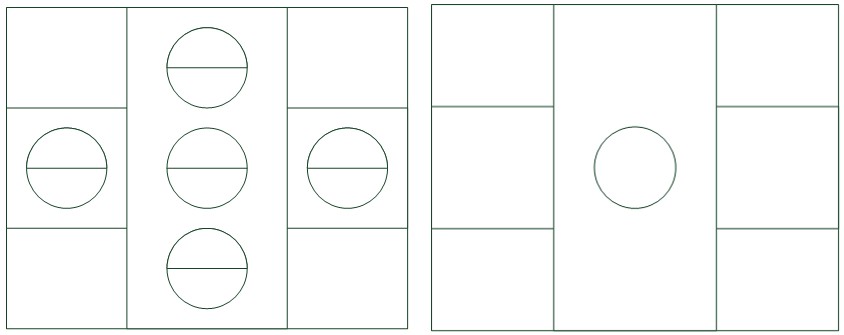
For example, the hypothesis Inspection methods, as shown in Figure 1, shows five holes are found, but it is only one true hole defect. The defect counts on pattern inspections are various by the die-to-database of the inspection sensitivity settings. This action to find hole patterns could has the difficult on the problems for die-to-die inspections. There could connect a lower-level metal to an upper-level metal. Due to the large leakage, it maybe causes the second electron or weaker beam reflects and other images could happen on somewhere. When it compares the transmitted images of two neighboring dies, some complicated features, such as, could cause virtual defects especially for the high circuit of e-beam machines. An inspection method of die-to-database then can be used for the comparison of the difference. Therefore, the database could be increased due to the sensitivity settings for comparison of the die-to-die and die-to-database. Therefore, big data could useful to obtained with the die-to-die and die- to-database methods.
(a) (b) Figure 1: Schematic diagram shows the virtual hole patterns. (a) Virtual images without using die-to-database method. (b) Only true hole is located on the central one using combining method.
Conclusion
Preparing semiconductors are briefly reviewed. Subsequent, the e-beam to view the defects for mask and wafer are also assess. The inspections are merging the die- to-die method and the die-to-database method proposed. Resultantly, big data will increase the defect counts, but using the big data technology could increase the precise of count and speed up the inspection time.
References
-
Levinson HJ (2021) Publication guidelines for metrology and masks. J Micro/Nanopattern Mater Metrol 20(2): 020101.
-
Chen YH (2020) Proceedings of the SMTA Pan Pacific Microelectronics Symposium, 1.
-
Miyai H, Kohyama T, Suzuki T, Takehisa K, Kusunose H (2020) Photomask Photomask BACUS 36(1): 11148.
-
Mochi I, Kim HS, Locans U, Dejkameh A, Nebling R, et al. (2020) Illumination control in lensless imaging for EUV mask inspection and review. Proc of SPIE 11323(11): 1132311.
-
Mochi I, Fernandez S, Nebling R, Locans U, Rajeev R, et al. (2020) Quantitative characterization of absorber and phase defects on EUV reticles using coherent diffraction imaging. J of Micro/Nanolithography, MEMS and MOEMS 19(1): 014002.
-
Broadbent W, Yokoyamab I, Yu P, Sekid K, Nomurad R, et al. (2007) Field results from a new die-to-database reticle inspection platform. Proc of SPIE 6607(14): 660714.
-
Alcaire T, Cunffa DL, Tortaib JH, Soulan S, Gredya V, et al. (2021) Detection and correlation of yield loss induced by color resist deposition deviation with a deep learning approach applied to optical acquisitions. Proc of SPIE 11611(35): 116112G.
-
Broadbent WH, Wiley JN, Saidin ZK, Watson SG, Alles DS, et al. (2004) Results from a new die-to-database reticle inspection platform. Proceedings of SPIE 5446.
- Solution-Processed Chiral Perovskites for Biomedical Applications
- Nanotechnology in Health Chemistry and Medicine: Current Challenges and Future Directions
- Human Exposure to Micro- and Nanoplastics: Pathways, Toxicity, and Intervention Strategies
- Exosome Nanomedicine for Cancer Therapy
- Micro and Nanoplastics–Plastisphere, Biotoxicity, Impact on Human Health, and Mitigation Strategies
- Process Validation of Cefixime Powder for Suspension Dosage Form, 50 mL