Certain Amount of Hydrogenthin Films Well-Si1-Xgex : H (X = 0 ÷ 1) for Electronic Devices
The possibilities of application of the technology of plasma-chemical deposition of films as well-Si1-xGex : H (x = 0 ÷ 1), undoped and doped with PH3 and B2H6, for use in the p-i-n- structures of solar cells. The optical properties, in the same defined amount of hydrogen contained in the film. It was found that the film properties greatly depend on the composition and the level of hydrogenation. The amount of hydrogen atoms in the films was varied by changing the gas mixture composition and IR absorption were measured for the films a-Si: H and a-Ge: H. Films based on a-Si: H and a-Si0,88Ge1,2: H solar cells are made from three layers of 1.3 cm2 area and cell efficiency ( ξ ) of 9.5%.
Introduction
Si alloy film and have different structural phases. The most interesting, are in an amorphous matrix of them are crystalline grains. Such alloys are manufactured by various methods and under various process conditions. For films of amorphous hydrogenated silicon a-Si: H, formed by cyclic deposition annealing in a hydrogen plasma, the effect Staeblera-Wronski is weak [1]. Golikova OA, et al. [2] also noted the virtual absence Staeblera-Wronski effect in nanostructures films as-Si: H. Crystallization films and silicon-Si: H is carried out by various methods: prolonged annealing in vacuum at 600˚S, rapid thermal processing [3], the laser annealing [4] and ion implantation [5]. Mobility of charge carriers and the efficiency of doping in these films is higher than in the a-Si: H, and the optical absorption coefficient higher than that of crystalline silicon. Films and xGex-Si1-: H, a-Si1-xSx: H are effective and cheap material for the manufacture of solar cells and other electronic devices [6, 7]. Therefore these films of receiving and changing their conductivity type are urgent tasks. In Colder H, et al. [8], with the change that the substrate temperature is increased Nano crystal growth. It was found that the average grain size (d) and the proportion of crystal grain volume (Vc) decreases with increasing concentration of PH3. When doped with boron, increasing B2H6 concentration value (d) does not change, and Vc decreases. Passivation properties and hydrogen-Ge: H worse than a-Si: H, so in general the films and fotoeffektivnost-Si1-xGex: H, somewhat lower than in a-Si: H [9, 10, 11].
Hydrogen atoms, and play an important major role in the structure of the film. The purpose of this work - is to determine the amount of hydrogen in the film and measuring its electro-physical properties, as well as the creation of electronic devices based on the films and Si$_{1-x}$Ge$_x$: H (x = 0 ÷ 1).
**Experimental Part**
Thin films of a-Si$_{1-x}$Ge$_x$: H (x = 0 ÷ 1) obtained by plasma deposition using gaseous mixtures of H2 + SiH4, He + GeH4 in various proportions. Details of the preparation of films shown in [12, 13]. The plasma is created by RF field mainly inductive coupling. The film thickness was 0,1 ÷ 1,0 mm. Measured absorption coefficient (à), refraction (n), reflection (R), transmission (T), the band gap (E) for each sample, using the Tauc model [14]. The optical absorption was studied at room temperature as described in [15, 16] 21-IR spectrometer.
**Results and Its Discussion**
The concentration of hydrogen in the films as-Si$_{1-x}$Ge$_x$: H, (x = 0 ÷ 1) is determined by the method of Abasov FP [15, 16]:
$$N = \frac{AN_A}{(\bar{A}/\xi)} \int \frac{\alpha(\omega)}{\omega} d\omega$$ (1),
Where, Avogadro number of N- and (D / £) integral force hydride with the unit cm$^2$/mol (H / $\xi$) = 3,5. If the absorption width is denoted by Aw and the center frequency 00, then when $\bar{A}u$ / $\omega$ 0 ≤ 0,1, after approximation with an accuracy of ± 2%, the equation (2) can be written as follows:
$$N = \frac{AN_A}{(\bar{A}/\xi)\omega_0} \int \frac{\alpha(\omega)}{\omega} d\omega$$ (2),
Where: $\bar{A}$ - dielectric constant. For Si $\bar{A}$ = 12; Ge $\bar{A}$ = 16.
If in equation (3) before integration expression denoted by AS, and - the total absorption of stretching modes for each film, then in determining the concentration of hydrogen (NH) obtain a general expression in abbreviated form:
$$N_H = A_S J_S$$ (3),
Ratio AS - films for a-Si: H, is in the tension mode 1,4
- 10$^{20}$ cm$^{-2}$. The absorption coefficient (à) for said frequency (2100 cm$^{-1}$) is 8
- 10$^{-1}$ ÷ 3
- 10$^{20}$ cm$^{-1}$ with NH = 10$^{21}$ ÷ 7
- 2.1 10$^{22}$ cm$^{-3}$. For films as-Ge: H = 1,7
- AS 10$^{20}$ cm$^{-2}$. Clearly, equation (3), also describes an oscillating fashion in connection stretching films as-Si: H, a-Ge: H and a-Si${1-x}$Gex: H. Estimates of relative hydrogen bonding to the hydrogenated amorphous as-Si${1-x}$Gex: H:
$$p = \frac{N_{Si-H}}{N_{Ge-H}} \frac{x}{1-x}$$ (4),
NSi-H where and NGe-H - the hydrogen concentration in the a-Si: H and a-Ge: H (in cm$^3$). Equation (3) can be rewritten for (wagging mode) films and rocking fashion-Si: H and a-Ge: H. Thus the value of NSi-H and NGe-H determined from the equation (3) for the fashion swing in the following form:
$$N_H = A_W J_W$$ (5),
Where - the total absorption rocking fashion for films and-Si: H and a-Ge: H. For these films Aw = 1,6
- 1019 cm$^{-2}$ and Aw = 1,1
- 1019 cm$^{-3}$, respectively. Knowing NGe-H (where, for a film-Ge: H, Aw = 1,6
- 1019 cm$^{-2}$ and à = 5
- 101 cm$^{-1}$) to calculate the concentration of hydrogen in the NH and the film-Si$_{1-x}$Gex: H for expression:
$$N_H = N_{uge-H} \left\{ \int \frac{\alpha_1(\omega)}{\omega} d\omega \right\} \left\{ \int \frac{\alpha_2(\omega)}{\omega} d\omega \right\}$$ (6),
Where - number of connections defined by modes of oscillation in a clean well-Ge: H, whose value is calculated according to the equation (5). The second factor in the expression for NH (integral ratio of infrared absorption maxima) is stretching vibrational mode of the sample in a clean and well-Ge: H. To calculate the ratio using integrated peak corresponding Ge-H (2000 cm$^{-1}$) and a film-Si$_{1-x}$Gex stretching vibrational mode: H.
From these data we can estimate the strength of the oscillator in the film as well-Si$_{1-x}$Gex: H ratio:
$$\bar{A} = J_S / J_W$$,
Where, $J_S \approx J_S^+ + J_S^-$, $J_W \approx J_W^+ + J_W^-$.
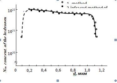
$J_S \approx J_S^+ + J_S^-$, $J_W \approx J_W^+ + J_W^-$. The values - $J_S^+$, $J_S^-$, $J_W^+$, $J_W^-$ are integral acquisitions fashion stretching and rocking fashion, respectively. Oscillator strength f = 0.51 (x = 0) and r = 0.13 (x = 1). The maximum value of P = 4.16 to x = 0.40. Table 1 shows the characteristic parameters of amorphous films a-Si$_{1-x}$Ge$_x$: H. Figure 1 shows the distribution of hydrogen across the film thickness d: 1-specific method of recoil protons 2 by infrared absorption spectrum. It can be seen that sufficiently uniform distribution of hydrogen. Note that the value of NH, defined by recoil protons (MOS) and IR spectroscopy agree within 2-3 atm (Figure 1).
The Optical Properties of the Films
Dependence on hν makes it possible to determine the width of the band gap [14, 16] for each film. In all the studied films of the optical absorption coefficient of the edge is described by the relation:
$$ \alpha h \nu = B \left(h \nu - E _ {0}\right) ^ {2} \tag {7}, $$
where = 5 ∙ 104 ÷ 105 cm-1, E0 is - optical bandgap for each film, In - proportionality factor. The value is determined depending on hν extrapolation for each sample. The quadratic dependence (7) obtained theoretically for Tauc model [14], which describes the density of states of the mobility gap. The value for x = 0 ÷ 1 is from 527 to 343 eV 1sm1 / 2, respectively, and for films-Si1-xGex: H (x = 0 ÷ 1) E0 = 1.14 ÷ 1.86 eV. We use the well-known relation, the absorption coefficient - is determined by the following equation [2, 4]:
( )( )( ) ( )
1 1 1 exp R R R d T R R R R R R R d α $$ T = \frac {\left(1 - R _ {1}\right) \left(1 - R _ {2}\right) \left(1 - R _ {3}\right) \exp (- \alpha d)}{\left(1 - R _ {2} R _ {3}\right) \left\{1 - \left[ R _ {1} R _ {2} + R _ {1} R _ {2} \left(1 - R _ {2}\right) ^ {2} \right] \right\} \exp (- 2} $$
1 2 3 (8) ( ) ( ) { } ( )
2 2 3 1 2 1 2 2
1 1 1 exp 2 α Here we assume that
2 2 2 2 1 0 0
( ) ( )
1 / 1 R n k n k $$ = \left| (n - 1) ^ {2} + k _ {0} ^ {2} \right| / \left| (n + 1) \right| ^ {2} + k $$
2 2 2 2 2 1 0 1 0
( ) ( ) / R n n k n n k $$ = \left| \left(n - n _ {1}\right) ^ {2} + k _ {0} ^ {2} \right| / \left| \left(n + n _ {1}\right) ^ {2} + k _ {0} ^ {2} \right| $$ (9)
2 ( ) ( )
1 / 1 R n n $$ = \left| \left(n _ {1} - 1\right) \right| / \left| \left(n _ {1} + 1\right) \right| $$
3 1 1 For weakly absorbing regions of the world.k0 shows light attenuation in the substrate. Note that the film thickness d, is determined in this case from the respective extreme transmission or reflection of the interference fringes.
From equation (8), the absorption coefficients are defined as follows:
$$ T = \frac {k x}{a \left(1 - b x\right) ^ {2}} \tag {10} $$
( )
2 1 Then,
2 , 4 2 ln , 4 1 2 . . 4
m d e k k mn m d k k mn m d k k mn α α $$ e ^ {- \alpha d} = \alpha = \frac {2 m}{k \pm \sqrt {k ^ {2} + 4}} $$
2 α $$ I = \ln \frac {2 m}{k \pm \sqrt {k ^ {2} + 4}} $$
(11)
2 α $$ t = \frac {1}{d}. \frac {2 m}{k \pm \sqrt {k ^ {2} + 4}} $$
2 Equation (11) is a working formula to determine the optical absorption coefficients for the films in weakly absorbing regions of the spectrum. In a strongly-absorbing regions of the spectrum, and. Then the equation (8) can be rewritten as follows: This formula is working to determine the optical absorption coefficient in strongly absorbing regions of the spectrum. Accordingly, the refractive indices are defined using. Or in the form of the following ( ) v c n dv α $$ - \int \left[ \frac {\alpha (v)}{v ^ {2}} \right] d v \tag {12} $$ $$ \ddot {A} n = \frac {c}{2 \pi^ {2}} \int \left[ \frac {\alpha (v)}{\nu^ {2}} \right] $$ π ν
Creating a Solar Cell
The research results show that the film and-Si1- xGex: H (x≥0,20) can be used as high-quality material in semiconductor electronics. For this purpose, we have developed a three-layer element based on a cascade-type dual-layer elements. The three-layer element is made of two-layer element consisting of two elements based on a-Si: H with p-i-n junction and the p-i-n element i- layer of a film-Si0,88Ge0,12: H. The thicknesses of the i- layers to the upper two transitions were selected so as to comply with the conditions of equality of short-circuit current of the lower element. Short-circuit current was about half the value for the element with one p-i-n junction. open-circuit voltage is increased, and short circuit current is reduced with increasing number of superimposed layers. This method can increase the number of layers (create an n-layered element). Note that for each item produced i- layer 0.5 microns thick. The area of each element was 1.3 cm2. When a three-layer solar cells must be observed uniform thickness and area of each element. The material of the substrate steel was chosen and used as a coating ZrO2 with 80% transmissivity. Covering ZrO2 simultaneously plays the role of the upper (front) contact. The thickness of the layers a-Si: H p- and n- type was about 300 and 400 Å, respectively.
For films doping amount of B2H6 and PH3 gas mixtures was varied between 0.1 and 0.5%, respectively. After deposition of the amorphous semiconductor layers deposited by evaporation ZrO2 film thickness of about 500 Å. Upper contacts used for Ni / Ag, to lower - stainless steel substrate. Items covered sunlight source provided AM-1 (100 mW / cm2). Short circuit current for sandwich elements was 8.5 mA / cm 2, the open circuit voltage of 2.25 ~ B, the filling factor of ~ 0.50 and n (efficiency) ~ 9.5% (Figure 3). Efficiency for single-layer and two-layer element element is 7% and 8.9%, respectively (Figure 2). Collection efficiency of carriers at different wavelengths is defined as:
( ) ( ) ( )
Ö J Y eN
$$ (\lambda) = \frac {J _ {\mathrm {O}} (\lambda)}{e N (\lambda)} \tag {13} $$
Jf where ( λ ) is the density of the photocurrent (10 mA / cm2), N ( λ ) - the number of photons incident on a unit area per second, e- free charge carriers.
For elements with the above structures is calculated short-circuit current in the assumption of complete exhaustion of all-shells, in the absence of forward bias. Thus, the short-circuit current for the first, second and third elements is given by the following expressions:
01 1,24/ E
( ) ( ) ( )
$$ I _ {S c 1} = q \int_ {0} ^ {1, 2 4 / E _ {0 1}} (1 - R) N _ {p h} \exp \left(- \alpha_ {n} W _ {n}\right) \left[ 1 - \exp \left(- \alpha_ {1} W _ {1}\right) \right] d \lambda \tag {14} $$
1 1 1 0 1 exp 1 exp
02 1,24/ E
( ) ( ) ( )
$$ I _ {S c 2} = q \int_ {0} ^ {1, 2 4 / E _ {0 2}} (1 - R) N _ {p h} \exp \left(- 2 \alpha_ {n} W _ {n} - \alpha_ {1} W _ {1} - \alpha_ {p} W _ {p}\right) \left[ 1 - \exp \left(- \alpha_ {2} W _ {2}\right) \right] d \lambda $$
2 1 1 2 2 0 1 exp 2 1 exp (15),
03 1,24/ E
( ) ( ) ( )
Sc ph n n n n p p I q R N W W W W W W d α α α α α α λ = − − − − − − − − ∫
3 1 1 2 2 3 3 0 1 exp 3 2 2 1 exp (16).
Here, the field distribution within the layer, respectively, - the number of photons incident on the surface of the elements, - the reflectance of the film, - the absorption coefficient for each layer elements.
The open circuit voltage for the cascade elements with two and three transitions represented in the form:
$$ V _ {o c} \left( / / \right) = 0, 5 \left(E _ {0 1} + E _ {0 2}\right) \tag {17} $$ $$ V _ {o c} \left(\mathrm {I I I}\right) = 0, 5 \left(E _ {0 1} + E _ {0 2} + E _ {0 3}\right) \tag {18} $$ The duty cycle for all elements specified by the value of 0.5. Short-circuit current of the cascade element with two transitions is given by the smaller of the values or. Short- circuit current of the cascade element with three transitions is determined by the smallest value of, or.
Efficiency multijunction cascade elements is given by:
( ) ( ) $$ \eta (i) = 0, 5. 0, 5 \left(\sum_ {i} E _ {0 i}\right) \frac {I _ {S c} (i)}{P _ {i n}} \tag {19} $$
0 0,5.0,5 Sc i i in or 3 where - indicates the number of layers, - the power of the incident light on the surface of the elements, its value is 100 mV / cm2 [10] - respectively, the band gap for each j-th layer.
To improve the solar cell to ç is required to increase the number of layers to reduce the area of the elements, the choice of metal wires, metal contacts to reduce resistance and others.
Measurements of spectral sensitivity are usually produced with a constant white light illumination, the intensity of which corresponds to normal operating conditions (AM- 100 ~ 1 MW / cm2), simultaneously modulating element falls calibrated monochromatic radiation. The photocurrent and its dependence on the wavelength of monochromatic radiation are measured in the shorted circuit with the help of a synchronized amp (Figure 3).
To determine the effectiveness of gathering important knowledge of the electric field that is transmitted to the element. It has been observed that the device configuration dependent collection efficiency is shifted from the red light in the blue region of the spectrum. The wavelength dependence of the number of photons is calculated using equation (27). It is known that the photon energy and momentum of the corresponding electromagnetic waves with a frequency and wavelength in a vacuum, are:
$$ W = h v = \frac {h c}{\lambda}; P ^ {*} = \frac {h v}{c} = \frac {h}{\lambda}, $$ where, h- Planck’s constant. When Malia frequencies - the predominant role played by the wave properties at high - corpuscular properties of light. Photoelectric effect (photoelectric effect) is the process of interaction of electromagnetic radiation with matter, in which the energy of the photon is transferred to an electron of an atom of matter. In addition, these properties of substances exist mechanical action produced by electromagnetic waves in the fall for what is called a surface pressure of light. If - energy electromagnetic radiation normally feed on a surface of unit area per 1 sec, c is the velocity of propagation of light waves in a vacuum, R- coefficient of surface reflection of light, the pressure P - light on the surface is equal to:
$$ P = \left(1 + R\right) N \frac {h v}{c} = P ^ {*} / c \left(1 + R\right) [ 2 0 ], $$ light pressure (P) is given by equation (19) and is denoted in the following form:
$$ P ^ {*} = \frac {W}{S} = \frac {h c}{\lambda S} \frac {N}{t} (2 1), $$
N- Number of incident photons at the time. W-energy photon incident on all the wavelengths of the body surface. P* - a pulse of light falling on the surface of 1cm2 for 1 sec. Then the force of the incident light is determined by the pressure in the following form:
$$ F = P \cdot S $$
( ) 1 (1 hcNS R hN R F Stc t λ λ $$ ' = \frac {h c N S (1 + R)}{\lambda S t c} = \frac {h N (1 + R)}{\lambda t} \tag {22} $$ $$ F \lambda t = h N \left(1 + R\right) $$
F - Light pressure force (F = 10-8H) on the surface (S = 1cm2),
- the length of the incident wave, h - Planck’s constant - the fall
of light for 1 sec, with energy and its value is NHN - photons,
with each impulse photon is hn / c. On reflection radiation
- and wavelength, the number of incident photons is 1017 ÷
1018 m-2s-1, 0,2 ÷ 0,8; = 300 ÷ 900 nm. - Reflects the ability
of the elements at 300 ÷ 900 nm. It is also possible with other
means to determine the number of photons:
$$ P = \frac {A}{t} = \frac {N h \gamma}{t} \tag {28} $$
Here, the work function of the A-rays of light in the fall and is, the P power light radiation and is 100 mW / cm2. From (22) we can determine the number of photons in the following form:
p t N hc λ = (29), Example:
Nanomedicine & Nanotechnology Open Access
$$1) N = \frac{F\lambda t}{h(1 + 0, 2)} = \frac{10^{-8} \hat{I} \cdot 9 \cdot 10^2 \cdot 10^{-9} i}{6, 62 \cdot 10^{-34} \hat{a}e \cdot \hat{n}a\hat{e} \cdot 1, 2} = 1, 3 \cdot 10^{17} \hat{o}i\hat{o} / i^2 \hat{n}$$
$$2) N = \frac{F\lambda t}{h(1 + 0, 8)} = \frac{10^{-8} \hat{I} \cdot 3 \cdot 10^2 \cdot 10^{-9} i}{6, 62 \cdot 10^{-34} \hat{a}e \cdot \hat{n}a\hat{e} \cdot 1, 8} = 10^{18} \hat{o}i\hat{o} / i^2 \hat{n}$$
Conclusion
By plasma deposition using gas mixtures H2 + SiH4; H2 + GeH4 obtained in different proportions and thin film-Si1-xGex: H (x = 0 ÷ 1). It is shown that the absorption coefficient for visible light and the bandgap increases with increasing silicon content. The carrier mobility in the film photoconductivity and a-Si: H is greatly reduced when a germanium content of 40 at%. Films based on a-Si: H and a-Si_{0.88}Ge_{0.12}: H solar cells are made and established monolayer, two-layer and three-layer structure; measure their performance. It was found that for single, double and triple layer structures with an area of 1.3 cm2 element $\varphi$ is 7; 8.9; 9.5%, respectively. For the three-layer cell collection efficiency peaks shifted to longer wavelengths. The structures obtained when illuminated by light in the wavelength range 0.3 ÷ 1.1 micron for 120 hr, No degradation was observed. It is shown that the structure of the solar cells on the basis of well-Si_{0.88}Ge_{0.12}: H and a-Si: H are effective and further efforts to improve the quality of films and higher-efficiency of the NIJ They are urgent tasks.
References
-
Afanasyev VP, Gudowski AS, Nevedomsky VN (2002) The effect of heat treatment on structure and properties of the films as well-Si: H, obtained by cyclic deposition 36: 238-243.
-
Golikova OA, Kazanin MM, Kudoyarova VH (1998) Effect Staeblera-Wronski, depending on the position of the Fermi level and the structure of undoped amorphous hydrogenated silicon 32: 484-489.
-
Mezdragina MM, Abramov AV, Macina GM, et al. (1998) Effects of the atomic hydrogen in the annealing atmosphere on the properties of amorphous hydrogenated silicon films and the parameters p-i-n structures on their basis. 32(5): 620-637.
-
Golikova OA, Babahodzhaev US (2002) Crystallization of amorphous hydrogenated silicon films deposited at different conditions 36: 1259-1262.
-
Golikova OA, Kuznetsov AN, Kudoyarova VH, Kazanin MM (1997) Features of the structure of amorphous hydrogenated silicon films deposited by the decomposition of silane at a constant current in the magnetic 31: 816-819.
-
Jones’ Pulos J, Lyukovski JM (1998) The physics of hydrogenated amorphous silicon. pp: 447.
-
Najafov BA (2006) Amorphous and microcrystalline semiconductors. Coll. tr. International Conf. St. Petersburg: Publishing House of the Polytechnic. Univ.
-
Colder H, Rizk R, Morales M, Marik P, Vicens J, et al. (2005) Influence of substrate temperature on the growth of nanocrystalline silicon carbide in reactive magnetron sputtering. J Appl Phys 98(2): 44-49.
-
King RR, Zaw DC, Edmontson KM, Fetzer CM, Kinzey GS, et al. (2007) Metamorphic multijunction solar cells GalnP / GalnAs / Ge with an efficiency of 40%. Appl Phys Lett 90(18): 231-239.
-
Hamakavy Y (1986) Amorphous semiconductors and devices based on them Metallurgy. pp: 374.
-
Najafov NA, Abasov FP (2014) Obtaining thin films for the creation of solar cells “PHOTONICS” 2(44): 72-90.
-
Abasov FP (2014) Influence of gamma radiation on electrik proportion of silicon solar cells. International journal of Pure and Applied Science and Technology 21(1): 12-16.
-
Abasov FP (2014) Effect of gamma irradiation on electrophysical and photoelectric parameters of double-barrier structure based on silicon. Nuclear Science and its ApplicationVII Eurasian Conference Baku 46(24): 233.
-
Abasov FP (2016) Effect of Gamma Irradiation on Photoelectric Parameters of Double-Barrier Structure Based on Silicon. Journal of Material Sciences and Engineering. USA 5: 269.
-
Abasov FP (2016) Study of radiation effects on photoelectric and luminescence parameters of two-barrier structures based on silicon. 2nd International Conference on Condensed Matter physics which is going to be held on October 26-28, in Chicago, USA.
-
Abasov FP (2016) Determining the amount of hydrogen in thin films well for solar cells. International Journal of Scientific Research in Engineering 1(1): 01-14.
- Solution-Processed Chiral Perovskites for Biomedical Applications
- Nanotechnology in Health Chemistry and Medicine: Current Challenges and Future Directions
- Human Exposure to Micro- and Nanoplastics: Pathways, Toxicity, and Intervention Strategies
- Exosome Nanomedicine for Cancer Therapy
- Micro and Nanoplastics–Plastisphere, Biotoxicity, Impact on Human Health, and Mitigation Strategies
- Process Validation of Cefixime Powder for Suspension Dosage Form, 50 mL