Interfacial Charge Transfer Processes in Perovskite-based Materials
Perovskite-based materials have gained significant attention in the last few years both in nanotechnology and optoelectronic applications. The interface between perovskites and electron (or hole) transport layers (ETL or HTL) plays a critical role in the charge transport properties in perovskite-based devices which eventually govern the final efficiency of the device. Therefore, it is extremely important to understand the interfacial charge transfer/transport processes in these materials. In this minireview, we summarize the ultrafast interfacial charge transfer processes from perovskites to electron/hole quenchers and highlight the importance of the surface coupling of such quenchers on the charge transfer and solar cell efficiency. A few examples of ETL and HTL and their effect on the device performance have been discussed. Therefore, the review will provide a platform to understand the importance of interfacial charge transfer processes and their effect on the final device efficiency in perovskite-based materials.
Introduction
Lead-halide perovskites have gained significant attention in the last few years due to their easy solution processability and interesting optoelectronic properties [1, 2, 3]. This leads to their multi-dimensional use in solar cell technology, light-emitting diodes (LEDs), photocatalysis, etc [4, 5, 6]. Perovskite-based thin-film solar cell was first demonstrated by Miyasaka and co-workers in 2009 where power conversion efficiency (PCE) of 3.8% was reported [7]. Since then research on perovskite-based materials has expanded in several dimensions. Lead-halide perovskites have ABX3 crystals structure where A is a monovalent organic or inorganic cation, usually occupying the octahedral void; B is divalent cation (e.g. Pb2+) and takes the body center of the octahedral; while the corners of the octahedral are occupied by the X- anion, usually halides (Figure 1a). One of the intriguing property of lead-halide perovskites is easy halide exchange leading to color tunable optical properties in the entire visible region [8]. Such unique properties make them ideal candidates for low-cost and high-efficiency photovoltaic and optoelectronic technology.
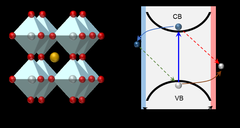
While using semiconductors in optoelectronic devices, e.g. solar cells or LEDs, it is extremely important to understand and tailor the interfacial charge transport properties [9, 10, 11, 12, 13]. The electron (and hole) transport properties are found to be the limiting factors in perovskite-based devices for the final efficiency [14, 15]. Therefore, the researcher came up with the idea of using electron and hole transport layers (ETL and HTL) on top of the perovskites to accelerate the charge transport processes along with the suppression of detrimental carrier recombination (Figure 1b) [16, 17, 18]. For example, in 2012, Park et. al. reported using a sub-micron thick TiO2 layer as ETL, MAPbI3 as a perovskite absorber, and 2,2′,7,7′-tetrakis (N,N-di-p-methoxyphenylamine)-9,9′- spirobifluorene (spiro-OMeTAD) as HTL [19]. The usage of ETL and HTL enables faster electron and hole transport through the interface, giving rise to as high as 9.7% PCE along with 500 h ambient air stability. Although the use of ETL and HTL was found to be beneficial for overall performance in photovoltaics, however, the interface between perovskite and ETL/HTL may limit the charge transport properties. Importantly, how the electron and hole quencher couple to the perovskite surface and how such surface coupling modulates the charge transfer processes needs to be understood equally. In this mini-review, we summarize interfacial charge transport processes in perovskite-based heterostructures, which often take place in ultrafast timescales. The surface coupling mechanism of electron/hole quencher and the consequent effect on charge transfer and PCE have been discussed. A few examples of ETL and HTL and their effect on PCE have been discussed. Overall, we think the review will provide a very good platform for researchers to understand the importance of the interfacial charge transport properties for optoelectronic applications.
Charge Transfer Dynamics at Different Interfaces
While device fabrication with perovskites, the interface plays an important role through which charge transfer occurs. It is therefore extremely important to understand the charge transfer processes across interfaces in perovskites, which take place in ultrafast timescale. Researchers have attempted several studies in the last few years to address the ultrafast interfacial charge transfer processes in different perovskite-based heterojunctions [20, 21, 22]. One of the early works on such interfacial charge transfer phenomenon was reported by the Lian group, where ultrafast interfacial electron and hole transfer dynamics from CsPbBr3 QDs was demonstrated, using femtosecond transient absorption (TA) spectroscopy (Figure 2a) [20]. Here benzoquinone (BQ) was used as an electron quencher while phenothiazine (PTZ) was used as a hole quencher. Figure 2b shows the UV-vis absorption and PL spectra of CsPbBr3 QDs while Figure 2c represents the corresponding TA spectra at indicated time delays. The TA spectra show a strong negative ∆A signal (bleaching), overlapped with the exciton absorption due to phase-space-filling of electrons and holes. Figure 2d compares the transient kinetics at the bleach maxima of CsPbBr3 QD without and with a quencher (the top panel is for BQ and the bottom panel is for PTZ). As can be clearly seen, upon the addition of both electron and hole quencher, the bleach recovery becomes much faster than the free CsPbBr3 QDs. It is important to note that this observation is in contrast to classical QDs (e.g. II-VI) where electron quencher makes faster bleach recovery while hole quencher slows down the bleach recovery kinetics [23]. This is because, in classical QDs, electrons mostly contribute to the absorption bleaching, however, in perovskites both electrons and holes contribute to the bleaching. The corresponding electron and hole transfer time to BQ and PTZ sensitized CsPbBr3 QDs is determined to be 65 and 49 ps, respectively. The faster interfacial charge transfer properties are the key to using perovskites in light harvesting and emitting devices.
In a recent example, we functionalize CsPbX3 NCs, where X= Cl, Br, I, with a bidentate 8-hydroxyquinoline (HQ) molecule that acts as a hole quencher [24]. Figure 2e shows the PL spectra of CsPbCl3 and CsPbI3 NCs without and with HQ molecule. The PL of CsPbCl3 NCs quenches completely upon functionalize with 4 mM HQ molecule. In contrast, the PL spectra of CsPbI3 NCs remain unaltered upon functionalization with the same concentration of HQ molecule. The PL quenching in CsPbCl3 NCs has been attributed to a thermodynamically viable interfacial charge (hole) transfer process, while no such charge (hole) transfer is active in CsPbI3 NCs. The corresponding interfacial hole transfer time in the CsPbCl3/HQ sample was estimated to be ~540 fs via probing transient bleach kinetics where faster bleach recovery was observed for the CsPbCl3/HQ sample than free CsPbCl3 NCs (Figure 2f). TA measurement further provides hole transfer time of ~2 ps in CsPbBr3/HQ system.
A microscopic surface coupling mechanism underlying the CT behavior in these NCs has been proposed via Fourier transform infrared spectroscopy as schematically depicted in Figure 2g. Here in CsPbCl3 (and CsPbBr3), the HQ molecule couples by forming halogen-hydrogen bonding between the two systems, which act as a CT bridge and promote the interfacial hole transfer process. In contrast, chelation was observed in CsPbI3/HQ material where both –N and –O from the HQ molecule simultaneously couple with Pb2+ in CsPbI3 NCs and restrict the CT process. Thus the work demonstrates the fundamental importance of the surface coupling of charge transport layers for efficient interfacial charge transfer processes.
![Figure 2: a) Schematic illustration of CsPbBr3 NCs-Benzoquinone (and Phenothiazine) complexes and possible interfacial charge transfer and recombination pathways. b) UV-vis absorption and PL spectra of CsPbBr3 NCs. c) TA spectra of CsPbBr3 NCs upon 400 nm laser excitation at a few different time delays. d) Comparison of exciton bleach recovery kinetics of CsPbBr3 NCs-BQ and CsPbBr3 NCs-PTZ complexes. e) PL spectra of free and HQ-functionalized CsPbCl3 (top) and CsPbI3 (bottom) NCs. For CsPbCl3 NCs, increasing HQ concentration (0 to 4 mM) is shown. f) TA kinetics at the bleach maxima of free and HQ- functionalized CsPbCl3 NCs. g) Schematic of interfacial charge transfer between CsPbCl3 NCs and HQ molecule via Cl-H bond, acting as a CT bridge (left), while no CT is active in the HQ-chelated CsPbI3 NCs (right). Reproduced with permission from (a-d) and (e-g) [20,24]. Copyright 2015, 2023 American Chemical Society.](/fulltextimages/11039/fig_2.png)
Figure 2: a) Schematic illustration of CsPbBr3 NCs-Benzoquinone (and Phenothiazine) complexes and possible interfacial charge transfer and recombination pathways. b) UV-vis absorption and PL spectra of CsPbBr3 NCs. c) TA spectra of CsPbBr3 NCs upon 400 nm laser excitation at a few different time delays. d) Comparison of exciton bleach recovery kinetics of CsPbBr3 NCs-BQ and CsPbBr3 NCs-PTZ complexes. e) PL spectra of free and HQ-functionalized CsPbCl3 (top) and CsPbI3 (bottom) NCs. For CsPbCl3 NCs, increasing HQ concentration (0 to 4 mM) is shown. f) TA kinetics at the bleach maxima of free and HQ- functionalized CsPbCl3 NCs. g) Schematic of interfacial charge transfer between CsPbCl3 NCs and HQ molecule via Cl-H bond, acting as a CT bridge (left), while no CT is active in the HQ-chelated CsPbI3 NCs (right). Reproduced with permission from (a-d) and (e-g) [20, 24]. Copyright 2015, 2023 American Chemical Society.
Importance of Surface Coupling on PCE
In fact, there are reports where researchers use such molecular coupling to passivate the surface trap states of perovskite, which eventually reduces the non-radiative losses, and has direct consequences on the solar cell performance. Snaith group demonstrates that in solution processes hybrid perovskites exhibit surface trap states due to uncoordinated surface Pb atoms within the crystal (Figure 3a) [25]. Photoexcited electrons may fall into these Coulomb traps, providing a major loss channel for the device. To control the loss, they come up with an idea of surface passivation of perovskites with Lewis bases, e.g. thiophene and pyridine, which can directly donate electron density to these defects (Figure 3b). Such treatment enhances the lifetime of perovskite by an order of magnitude (~2 ms), which they propose due to electronic passivation of the uncoordinated surface Pb atoms. This leads to an enhancement of perovskite- based hetero junction’s stabilized solar cell efficiency from 8.3% to 14.1% and 15.5% upon thiophene and pyridine treatment, respectively (Figure 3c & 3d).
In another example, they show uncoordinated surface iodine ions introduce trap states in perovskites, leading to surface charge accommodation and harmful charge recombination in the solar cell [26]. They used iodopentafluorobenzene (IPFB) for the surface treatment of MAPbI3 perovskites, which passivate the surface hole trap states by supramolecular halogen bonding. Their time- resolved PL experiment suggests using HTL such as spiro- OMeTAD makes the PL decay of MAPbI3 slightly faster with the IPFB treated sample, indicating localization of holes at the spiro-OMeTAD (Figure 3e). No change in the PL decay was observed for IFPB treated and untreated samples without any OMeTAD. Moreover, nano-to-millisecond TA decay was measured in the IFPB-treated and untreated samples to understand the charge recombination dynamics at the perovskite/OMeTAD interface. While in the untreated sample, the recombination is much faster (300 ns), the IPFB treated MAPbI3 sample shows a much longer recombination timescale (~950 ns) (Figure 3f). As shown in Figure 3g, the uncoordinated surface iodide ions are acting as hole traps in the untreated sample. However, the TA result indicates that the hole lifetime increases more than three-fold in spiro- OMeTAD in the presence of IPFB, resulting in a significantly suppressed recombination process. This is due to the effective passivation of the uncoordinated surface iodide ions by IPFB via halogen bonding, which reduce the density of the charge accumulation at the interface (Figure 3h) and is beneficial for solar cell.
![Figure 3: a) Schematic showing loss of iodine leads to the creation of vacancy, resulting in a net positive charge on Pb atoms. Photoexcited electrons can fall into these Coulomb trap states, thus neutralizing the charges. b) Thiophene (or pyridine) molecule can donate electron density to the defects, and neutralize the excess positive charge in the crystal lattice. Stabilized efficiency of c) thiophene and d) pyridine-passivated devices. e) Time-resolved PL decay traces of MAPbI3 without and with Spiro-OMeTAD. Black and red lines indicate without and with IPFB treatment. f) Nanosecond TA decay traces of IPFB treated (red) and untreated (black) samples, following 500 nm excitation and probing at 640 nm. g) Illustration of electrostatic interaction of uncoordinated halide anions with the hole injected into the Spiro-OMeTAD. h) Electrostatic screening of halides by halogen bond formation of IPFB on perovskite surface. Reproduced with permission from (a-d) [25] and (e-h) [26]. Copyright 2014 American Chemical Society.](/fulltextimages/11039/fig_3.png)
Figure 3: a) Schematic showing loss of iodine leads to the creation of vacancy, resulting in a net positive charge on Pb atoms. Photoexcited electrons can fall into these Coulomb trap states, thus neutralizing the charges. b) Thiophene (or pyridine) molecule can donate electron density to the defects, and neutralize the excess positive charge in the crystal lattice. Stabilized efficiency of c) thiophene and d) pyridine-passivated devices. e) Time-resolved PL decay traces of MAPbI3 without and with Spiro-OMeTAD. Black and red lines indicate without and with IPFB treatment. f) Nanosecond TA decay traces of IPFB treated (red) and untreated (black) samples, following 500 nm excitation and probing at 640 nm. g) Illustration of electrostatic interaction of uncoordinated halide anions with the hole injected into the Spiro-OMeTAD. h) Electrostatic screening of halides by halogen bond formation of IPFB on perovskite surface. Reproduced with permission from (a-d) [25] and (e-h) [26]. Copyright 2014 American Chemical Society.
ETL (HTL)/Perovskite Interface Figure 4 represents a schematic presentation of commonly used ETL’s and HTL’s in perovskite solar cells [27]. The conduction (valence) band offset between ETL (HTL) and perovskite is around 0.2 eV. Such band offset allows efficient interfacial charge transport in perovskite-based devices. A typical device structure of a hybrid perovskite solar cell with HTL PEDOT: PSS and a polymer-based electron extraction layer is shown in Figure 5a [28]. Three different n-type polymers, e.g. P(NDI2OD-T2), P(NDI2DT-T2), and P(NDI2OD-TET), were used as electron extraction layers to understand the driving force of solar cell performance. The energy level alignment of these polymers with respect to the hybrid perovskite is shown in Figure 5b, indicating very similar alignment for three polymers having small energy offset between the conduction band minima of perovskite and the LUMO of polymers. Steady-state and time-resolved PL measurement shows efficient quenching of the perovskite PL upon conjugation with these polymers (Figure 5c&5d). While pure perovskite shows a lifetime of 21.2 ns, the lifetime reduces significantly to 4.8, 5.8, and 8.7 ns respectively for all three polymers. The PL quenching together with the energy level alignment suggests efficient interfacial electron extraction from perovskite to all three polymers. The solar cell device parameters from J-V characteristics show promising performance for P(NDI2OD-T2), and P(NDI2DT-T2) as electron extraction layer, with a PCE of ~11 % for both (Figure 5e). Surprisingly, negligible PCE of ~0.18% was observed with P(NDI2OD-TET), although the PL experiments show efficient interfacial electron extraction from perovskite in the presence of this polymer. Here the ethyl unit of P(NDI2OD-TET) decreases the conjugation, leading to bandgap widening and low carrier transport property. Importantly, the electron mobility measurement indicates more than three orders of lower mobility (10-8 cm2 V-1 s-1) in P(NDI2OD-TET) than the other two polymers. Therefore, the authors proposed electron mobility as the bottleneck of the device, rather than interfacial electron extraction efficiency. The results indicate the important role of charge extraction layers which is not limited to the efficiency of charge extraction from perovskites but also to the charge transport properties which are governed by the mobility of the charge carriers.
![Figure 4: Schematic band alignment of several electron and hole transport materials in perovskite solar cell. Reproduced with permission from [27]. Copyright 2021 American Institute of Physics.](/fulltextimages/11039/fig_4.png)
![Figure 5: a) A typical device structure of a hybrid perovskite solar cell. b) Energy levels of MAPb(I/Cl)3 and three n-type polymers P(NDI2OD-T2, P(NDI2DT-T2), and P(NDI2OD-TET). c) Steady-state spectra and d) time-resolved PL decay of MAPb(I/ Cl)3 without and with three n-type polymers. e) Parameters for solar cell performance of perovskites with three different electron extraction layers under AM 1.5 G 100 mW cm-2. Reproduced with permission from [28]. Copyright 2016 Royal Society of Chemistry.](/fulltextimages/11039/fig_5.png)
Figure 5: a) A typical device structure of a hybrid perovskite solar cell. b) Energy levels of MAPb(I/Cl)3 and three n-type polymers P(NDI2OD-T2, P(NDI2DT-T2), and P(NDI2OD-TET). c) Steady-state spectra and d) time-resolved PL decay of MAPb(I/ Cl)3 without and with three n-type polymers. e) Parameters for solar cell performance of perovskites with three different electron extraction layers under AM 1.5 G 100 mW cm-2. Reproduced with permission from [28]. Copyright 2016 Royal Society of Chemistry.
Conclusions
In conclusion, ultrafast interfacial electron and hole transfer dynamics have been summarized between CsPbBr3 perovskite NCs and electron/hole quenchers which are key properties for using perovskites in optoelectronic applications. We further demonstrate that the molecular coupling to the perovskite surface may govern the ultrafast CT properties significantly and may alter by tunning the halide content of the perovskites. It has been observed that surface vacancy created by uncoordinated Pb-atoms and halides may passivate by using suitable molecules that may act as a charge acceptor and contribute to the enhancement of the final efficiency. Finally, we summarize different ETL and HTL for efficient photovoltaic device fabrication, which shows that the role of ETL and HTL is not limited to charge extraction only. However, the critical role of charge transport properties, governed by the mobility of the transport layers, is equally important for the final efficiency. We believe this mini-review will provide a swift understanding of the critical ultrafast interfacial charge transport properties and surface coupling mechanism in perovskite heterojunction for improved solar cell efficiency, and may lead to the design of better perovskite architecture for improved photovoltaics and optoelectronic technology.
Acknowledgments
T.D. acknowledges the Department of Science & Technology (DST) and the Science and Engineering Research Board (SERB) for the Ramanujan Fellowship Award (RJF/2021/000125). We acknowledge Prof. P. K. Iyer, Director (officiating), IIT Guwahati for his encouragement. We sincerely thank Prof. A. Chattopadhyay, IIT Guwahati for his help, and encouragement.
Conflicts of Interest
The author declares no conflict of interest.
References
-
Dey A, Ye J, De A, Debroye E, Ha SK, et al. (2021) State of the Art and Prospects for Halide Perovskite Nanocrystals. ACS Nano 15(7): 10775-10981.
-
Protesescu L, Yakunin S, Bodnarchuk MI, Krieg, F, Caputo R, et al. (2015) Nanocrystals of Cesium Lead Halide Perovskites (CsPbX3, X = Cl, Br, and I): Novel Optoelectronic Materials Showing Bright Emission with Wide Color Gamut. Nano Letters 15(6): 3692-3696.
-
Tong Y, Bladt E, Aygüler MF, Manzi A, Milowska KZ, et al. (2016) Highly Luminescent Cesium Lead Halide Perovskite Nanocrystals with Tunable Composition and Thickness by Ultrasonication. Angewandte Chemie International Edition 55(44): 13887-13892.
-
Byranvand MM, Otero-Martínez C, Ye J, Zuo W, Manna L, et al. (2022) Recent Progress in Mixed A-Site Cation Halide Perovskite Thin-Films and Nanocrystals for Solar Cells and Light-Emitting Diodes. Advanced Optical Materials 10(14): 2200423.
-
Cao M, Damji Y, Zhang C, Wu L, Zhong Q, et al. (2020) Low-Dimensional-Networked Cesium Lead Halide Perovskites: Properties, Fabrication, and Applications. Small Methods 4(12): 2000303.
-
Garai R, Gupta RK, Tanwar AS, Hossain M, Iyer PK (2021) Conjugated Polyelectrolyte-Passivated Stable Perovskite Solar Cells for Efficiency Beyond 20%. Chemistry of Materials 33(14): 5709-5717.
-
Kojima A, Teshima K, Shirai Y, Miyasaka T (2009) Organometal Halide Perovskites as Visible-Light Sensitizers for Photovoltaic Cells. Journal of the American Chemical Society 131(17): 6050-6051.
-
Nedelcu G, Protesescu L, Yakunin S, Bodnarchuk MI, Grotevent J, et al. (2015) Fast Anion-Exchange in Highly Luminescent Nanocrystals of Cesium Lead Halide Perovskites (CsPbX3, X = Cl, Br, I). Nano Letters 15(8): 5635-5640.
-
Shao S, Loi MA (2020) The Role of the Interfaces in Perovskite Solar Cells. Advanced Materials Interfaces 7(1): 1901469.
-
Schulz P, Cahen D, Kahn A (2019) Halide Perovskites: Is It All about the Interfaces? Chemical Reviews 119(5): 3349-3417.
-
Luo C, Zheng G, Gao F, Wang X, Zhan C, et al. (2023) Engineering the buried interface in perovskite solar cells via lattice-matched electron transport layer. Nature Photonics 17: 856-864.
-
Begum R, Parida MR, Abdelhady AL, Murali B, Alyami NM, et al. (2017) Engineering Interfacial Charge Transfer in CsPbBr3 Perovskite Nanocrystals by Heterovalent Doping. Journal of the American Chemical Society 139(2): 731-737.
-
Zhou M, Sarmiento JS, Fei C, Wang H (2019) Charge Transfer and Diffusion at the Perovskite/PCBM Interface Probed by Transient Absorption and Reflection. The Journal of Physical Chemistry C 123(36): 22095-22103.
-
Green MA, Ho-Baillie A, Snaith HJ (2014) The emergence of perovskite solar cells. Nature Photonics 8(7): 506-
-
Grill I, Aygüler MF, Bein T, Docampo P, Hartmann NF, et al. (2017) Charge Transport Limitations in Perovskite Solar Cells: The Effect of Charge Extraction Layers. ACS Applied Materials & Interfaces 9(43): 37655-37661.
-
Lee MM, Teuscher J, Miyasaka T, Murakami TN, Snaith HJ (2012) Efficient Hybrid Solar Cells Based on Meso- Superstructured Organometal Halide Perovskites. Science 338(6107): 643-647.
-
Ball JM, Lee MM, Hey A, Snaith HJ (2013) Low- temperature processed meso-superstructured to thin- film perovskite solar cells. Energy & Environmental Science 6(6): 1739-1743.
-
Etgar L, Gao P, Xue Z, Peng Q, Chandiran AK, et al. (2012) Mesoscopic CH3NH3PbI3/TiO2 Heterojunction Solar Cells. Journal of the American Chemical Society 134(42): 17396-17399.
-
Kim HS, Lee CR, Im JH, Lee KB, Moehl T, et al. (2012) Lead Iodide Perovskite Sensitized All-Solid-State Submicron Thin Film Mesoscopic Solar Cell with Efficiency Exceeding 9%. Scientific Reports 2(1): 591.
-
Wu K, Liang G, Shang Q, Ren Y, Kong D, et al. (2015) Ultrafast Interfacial Electron and Hole Transfer from CsPbBr3 Perovskite Quantum Dots. Journal of the American Chemical Society 137(40): 12792-12795.
-
Maity P, Dana J, Ghosh HN (2016) Multiple Charge Transfer Dynamics in Colloidal CsPbBr3 Perovskite Quantum Dots Sensitized Molecular Adsorbate. The Journal of Physical Chemistry C 120(32): 18348-18354.
-
Fang Q, Qiuyu Shang, Liyun Zhao, Rui Wang, Zhepeng Zhang, et al. (2018) Ultrafast Charge Transfer in Perovskite Nanowire/2D Transition Metal Dichalcogenide Heterostructures. The Journal of Physical Chemistry Letters 9(7): 1655-1662.
-
Debnath T, Sebastian D, Maiti S, Ghosh HN (2017) Tuning Hole and Electron Transfer from Photoexcited CdSe Quantum Dots to Phenol Derivatives: Effect of Electron- Donating and - Withdrawing Moieties. Chemistry-a European Journal 23(30): 7306-7314.
-
Manna M, Pal S, Goswami T, Bhandari S, Debnath T (2023) Halide-Driven Halogen–Hydrogen Bonding versus Chelation in Perovskite Nanocrystals: A Concept of Charge Transfer Bridging. The Journal of Physical Chemistry Letters 14(2): 354-362.
-
Noel NK, Abate A, Stranks SD, Parrott ES, Burlakov VM, et al. (2014) Enhanced Photoluminescence and Solar Cell Performance via Lewis Base Passivation of Organic– Inorganic Lead Halide Perovskites. ACS Nano 8(10): 9815-9821.
-
Abate A, Saliba M, Hollman DJ, Stranks SD, Wojciechowski K, et al. (2014) Supramolecular Halogen Bond Passivation of Organic–Inorganic Halide Perovskite Solar Cells. Nano Letters 14(6): 3247-3254.
-
Pan H, Shao H, Zhang XL, Shen Y, Wang M (2021) Interface engineering for high-efficiency perovskite solar cells. Journal of Applied Physics 129(13): 30904.
-
Shao S, Chen Z, Fang HH, ten Brink GH, Bartesaghi D, et al. (2016) N-type polymers as electron extraction layers in hybrid perovskite solar cells with improved ambient stability. Journal of Materials Chemistry A 4(7): 2419- 2426.
- Solution-Processed Chiral Perovskites for Biomedical Applications
- Nanotechnology in Health Chemistry and Medicine: Current Challenges and Future Directions
- Human Exposure to Micro- and Nanoplastics: Pathways, Toxicity, and Intervention Strategies
- Exosome Nanomedicine for Cancer Therapy
- Micro and Nanoplastics–Plastisphere, Biotoxicity, Impact on Human Health, and Mitigation Strategies
- Process Validation of Cefixime Powder for Suspension Dosage Form, 50 mL